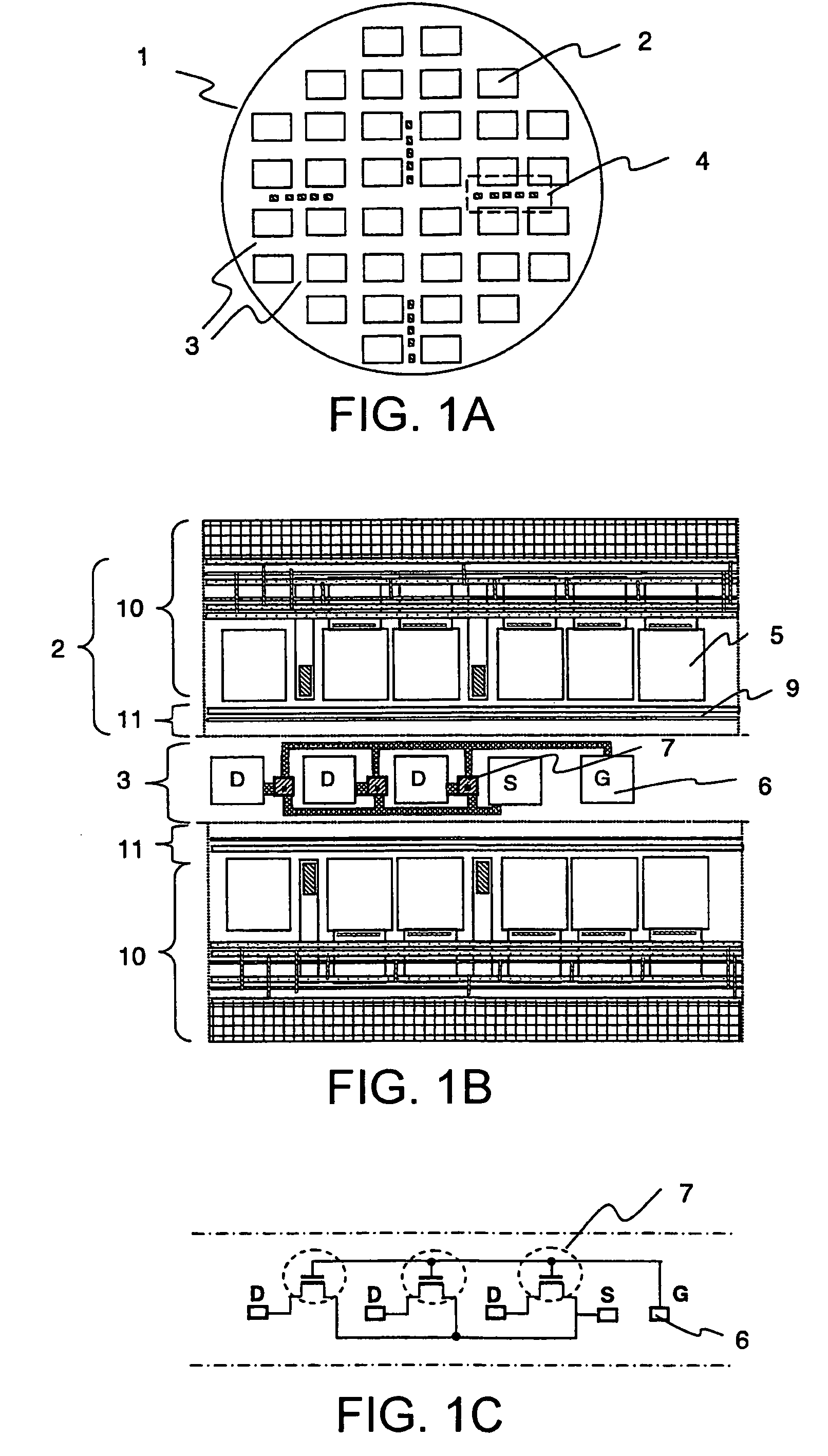
Semiconductor device
a technology of semiconductor devices and semiconductors, applied in the direction of semiconductor devices, semiconductor/solid-state device testing/measurement, semiconductor/solid-state device details, etc., can solve the problem of leakage of confidential and prevent leakage of information regarding semiconductor design and manufacture. , no cost increase of semiconductor devices is caused, the effect of preventing a leakage of information
- Summary
- Abstract
- Description
- Claims
- Application Information
AI Technical Summary
Benefits of technology
Problems solved by technology
Method used
Image
Examples
first embodiment
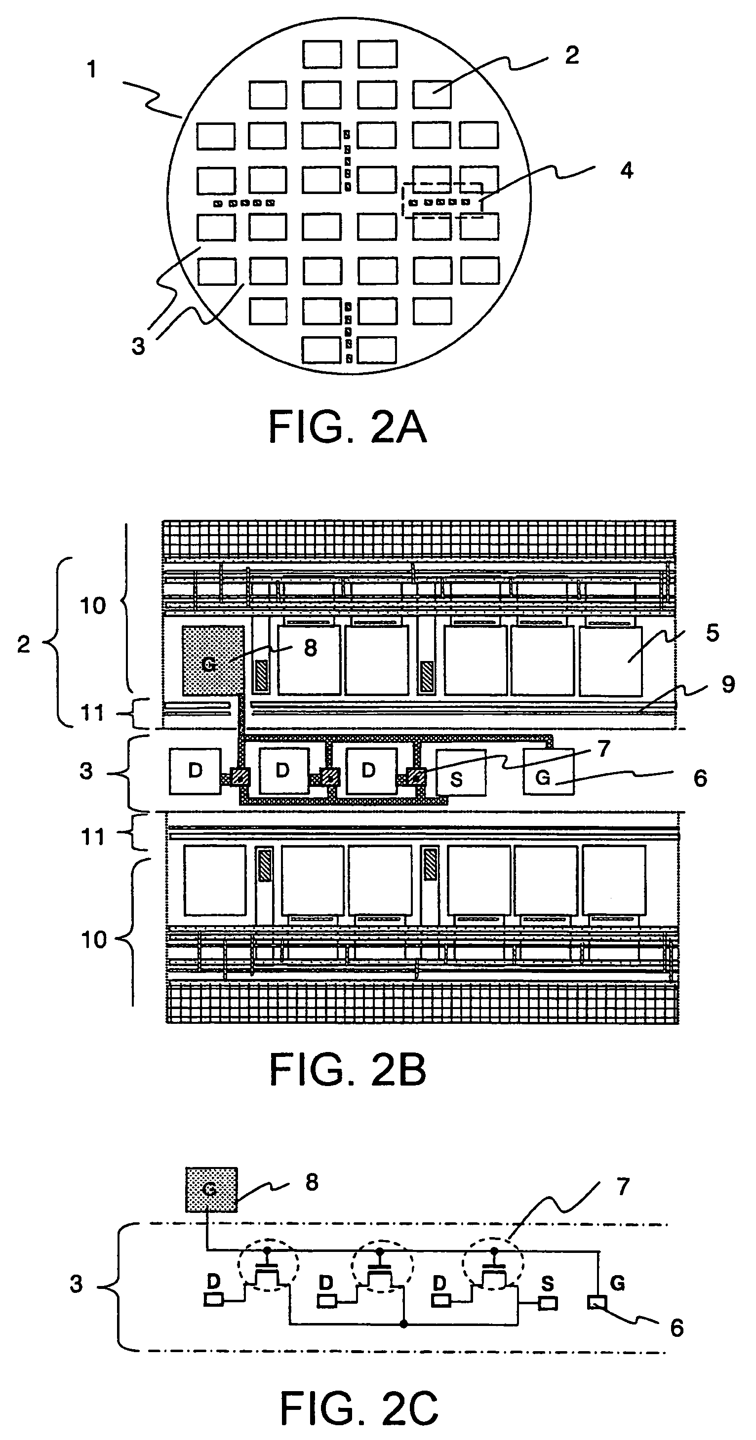
[0050]Referring to FIGS. 2 and 3, a semiconductor device according to a first embodiment of the present invention will be described. As a characteristic checking element of the first embodiment, three checking transistors are shown by way of example. FIGS. 2A, 2B, and 2C show a plan view of a wafer, a view showing a pad arrangement of the characteristic checking element, and a view showing connection of the checking transistors as the characteristic checking element, respectively. FIGS. 3A, 3B, and 3C show a plan view of the wafer, an enlarged plan view of a part of the wafer, and a sectional view of a sub-connection wiring taken along a line A-A′ in FIG. 3B, respectively.
[0051]On a wafer 1, a plurality of semiconductor devices 2 are arranged in a matrix fashion. Each of the semiconductor devices 2 has four sides surrounded by dicing lines 3. The dicing lines 3 for separating and segmenting the wafer 1 into the individual semiconductor devices 2 are formed in vertical and horizontal...
second embodiment
[0059]Referring to FIGS. 4 through 9B, a semiconductor device according to a second embodiment of the present invention will be described. As a characteristic checking element of the second embodiment, checking resistance elements are shown by way of example. It is difficult to break the checking resistance elements merely by applying an electric voltage. Therefore, in this embodiment, the checking resistance elements constituting the characteristic checking element are connected to an easily breakable transistor. FIGS. 4 through 8 are views showing first through fifth examples of circuit connections of the checking resistance elements, respectively. FIGS. 9A and 9B show arrangements of the checking resistance elements.
[0060]FIG. 4 is a view showing the first example of circuit connection in case where the characteristic checking element comprises the checking resistance elements. It is difficult to break the checking resistance elements merely by applying an electric voltage. There...
third embodiment
[0069]Referring to FIGS. 10A, 10B, 11A, and 11B, a semiconductor device according to a third embodiment of the present invention will be described. This embodiment shows connection between an internal measurement pad and a characteristic checking element in a wafer state. As the characteristic checking element, three checking transistors are shown by way of example. FIG. 10A is a plan view of a wafer and FIG. 10B is a connection diagram of a reticle for use in a photolithography process. FIGS. 11A and 11B show an embodiment in which the characteristic checking elements are connected to one another by the dicing line. FIG. 11A is a plan view of a wafer and FIG. 11B is a connection diagram of a reticle for use in the photolithography process.
[0070]Description will be made about connection of the characteristic checking elements 4 on the reticle 13 in FIG. 10B. On the reticle 13, the semiconductor devices 2 are disposed, nine in total, in three (top, middle, and bottom) horizontal rows...
PUM
 Abstract
Description
Claims
Application Information
 - R&D
- Intellectual Property
- Life Sciences
- Materials
- Tech Scout
- Unparalleled Data Quality
- Higher Quality Content
- 60% Fewer Hallucinations
Browse by: Latest US Patents, China's latest patents, Technical Efficacy Thesaurus, Application Domain, Technology Topic, Popular Technical Reports.
© 2025 PatSnap. All rights reserved.Legal|Privacy policy|Modern Slavery Act Transparency Statement|Sitemap|About US| Contact US: help@patsnap.com


