
Silicon material with controlled agglomerated point defects and oxygen clusters induced by the lateral surface

a technology of oxygen clusters and lateral surfaces, which is applied in the direction of silicon compounds, separation processes, and under a protective fluid, can solve the problems of intrinsic point defects not being mobile within commercially practicable periods of time, challenging restrictions imposed by microelectronic devices on the quality of silicon substrates, and numerically expensive numerical simulations based on predicting the size distribution of microdefect populations at every location in the crystal

Active Publication Date: 2014-03-18
GLOBALWAFERS CO LTD
View PDF117 Cites 26 Cited by
  • Summary
  • Abstract
  • Description
  • Claims
  • Application Information

AI Technical Summary

Benefits of technology

This approach results in single crystal silicon ingots and wafers with significantly reduced agglomerated intrinsic point defects, enhancing the quality and yield of semiconductor materials by minimizing defect formation and improving the radial uniformity of defect distribution.

Problems solved by technology

The continuously shrinking size of the modern microelectronic device imposes challenging restrictions on the quality of the silicon substrate, which is essentially determined by the size and the distribution of the grown-in microdefects.
Alternatively, a rigorous numerical simulation based on predicting the size distributions of the microdefect populations at every location in the crystal is numerically expensive.
First, defect “nucleation” occurs, which is the result of the intrinsic point defects being supersaturated at a given temperature; above this “nucleation threshold” temperature, intrinsic point defects remain soluble in the silicon lattice.
Below this “diffusivity threshold” temperature, intrinsic point defects are no longer mobile within commercially practical periods of time.
While the ingot remains above the “diffusivity threshold” temperature, vacancy or interstitial intrinsic point defects diffuse through the silicon lattice to sites where agglomerated vacancy defects or interstitial defects, respectively, are already present, causing a given agglomerated defect to grow in size.
Such defects are not responsible for gate oxide integrity failures, an important wafer performance criterion, but they are widely recognized to be the cause of other types of device failures usually associated with current leakage problems.
Agglomerated intrinsic point defects are therefore of rapidly increasing importance to device manufacturers, because such defects can severely impact the yield potential of the single crystal silicon material in the production of complex and highly integrated circuits.
Additionally, however, such approaches may involve controlling the subsequent thermal history of the crystal to allow for prolonged diffusion time to suppress the concentration of intrinsic point defects therein, and thus substantially limit or avoid the formation of agglomerated intrinsic point defects in a portion or all of the crystal.

Method used


Image

  • Silicon material with controlled agglomerated point defects and oxygen clusters induced by the lateral surface
  • Silicon material with controlled agglomerated point defects and oxygen clusters induced by the lateral surface
  • Silicon material with controlled agglomerated point defects and oxygen clusters induced by the lateral surface

Examples


Embodiment Construction

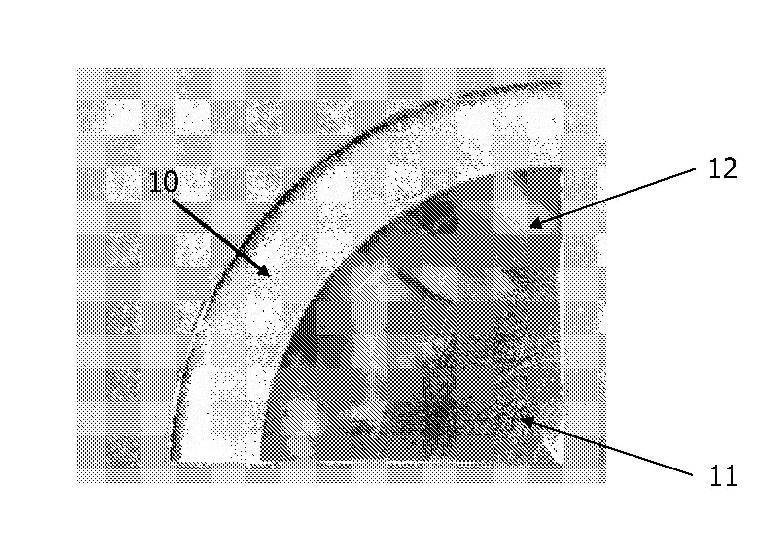
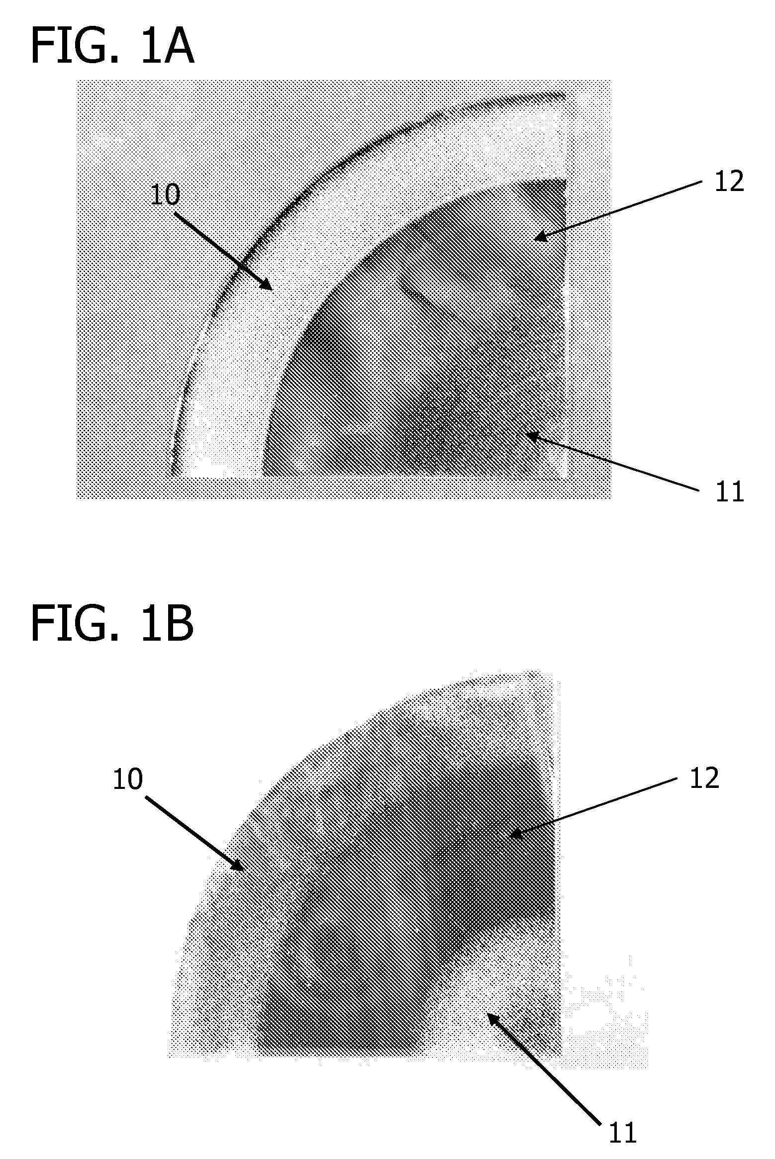
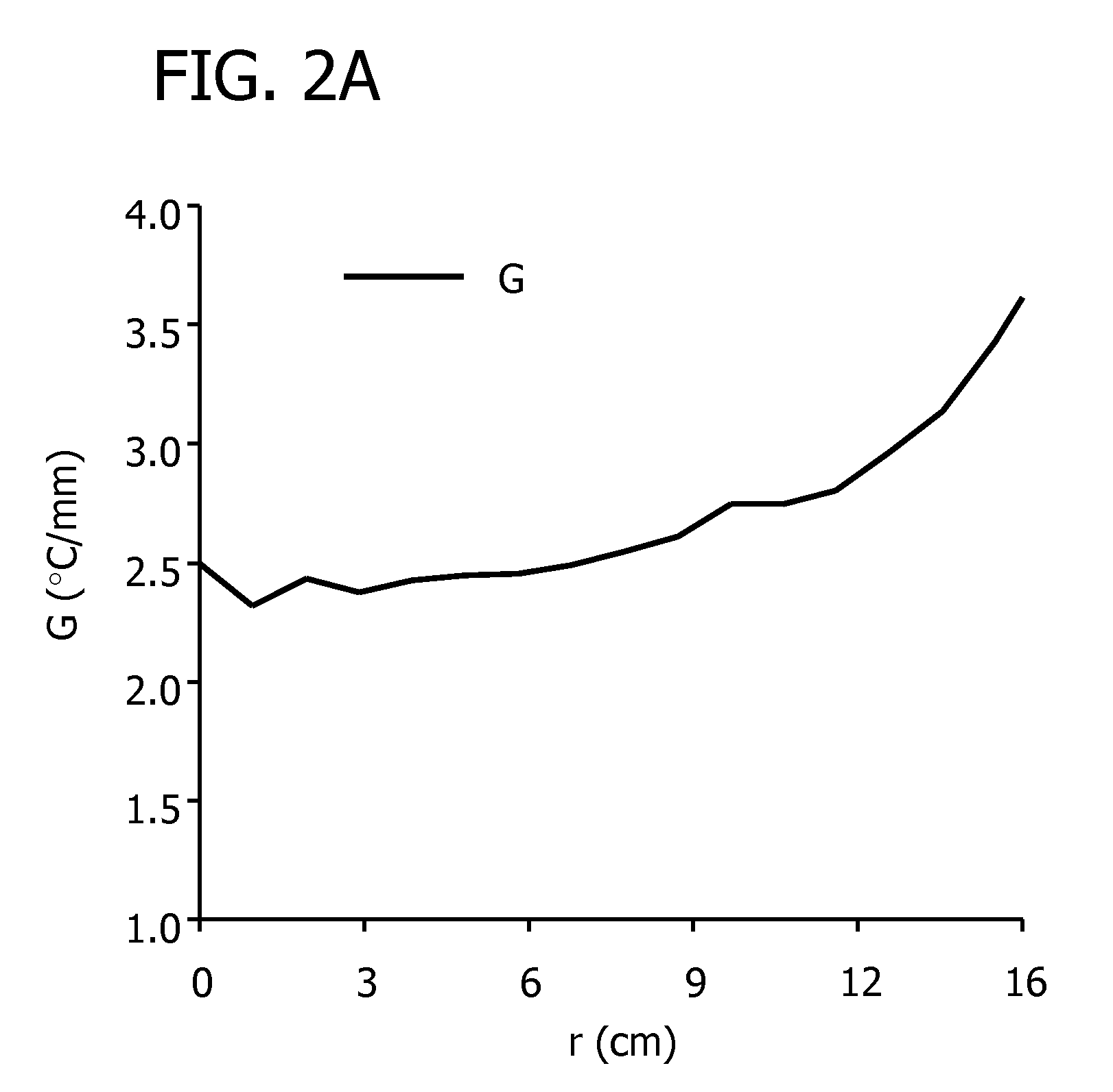
[0069]In accordance with the present invention, it has been discovered that, when attempting to grow a single crystal silicon ingot according to the Czochralski method under growth conditions such that at least a segment thereof is substantially free of agglomerated intrinsic point defects, an annular or peripheral ring (i.e., an “edge ring”) of some measurable width, which extends radially inward from about the lateral surface of the ingot, may be formed which contains agglomerated vacancy defects (i.e., “D-defects”) and / or oxygen clusters. More specifically, it has been discovered that, in a process for preparing a CZ single crystal silicon ingot, wherein the growth velocity, v, and the axial temperature gradient, G (or, as further detailed herein, more accurately the “corrected” or “effective” axial temperature gradient, “Gcorrected” or “Geffective”, respectively) are controlled such that, at a given axial position, the value of v / Geffective is substantially near the critical val...


PUM

PropertyMeasurementUnit
temperatureaaaaaaaaaa

Abstract

The present invention relates to a single crystal silicon ingot or wafer wherein the lateral incorporation effect of intrinsic point defects has been manipulated such that the formation of agglomerated intrinsic point defects and / or oxygen precipitate clusters in a ring extending radially inward from about the lateral surface of the ingot segment is limited.

Description

REFERENCE TO RELATED APPLICATIONS[0001]This application claims priority from U.S. provisional application Ser. No. 60 / 801,953 filed on May 19, 2006, the entire disclosure of which is incorporated herein by reference.BACKGROUND OF THE INVENTION[0002]The present invention generally relates to the preparation of semiconductor grade single crystal silicon which is used in the manufacture of electronic components. More particularly, the present invention relates to a Czochralski process for preparing single crystal silicon ingots which are substantially free of agglomerated intrinsic point defects, as well as wafers obtained therefrom.[0003]Single crystal silicon, which is the starting material for most processes for the fabrication of semiconductor electronic components, is commonly prepared by the so-called Czochralski (“CZ”) method. In this method, polycrystalline silicon (“polysilicon”) is charged to a crucible and melted, a seed crystal is brought into contact with the molten silico...

Claims


Application Information

Patent Timeline
Patent Type & Authority Patents(United States)
IPC IPC(8): C30B15/20C30B15/00C30B15/14
CPCC30B15/14C30B15/20C30B15/203C30B29/06C30B15/00C30B15/206H01L21/20
Inventor KULKARNI, MILIND, S.
Owner GLOBALWAFERS CO LTD
Learn More