Radiation image capturing device
a technology of radiation image and capture device, which is applied in the direction of radiation controlled devices, optical radiation measurement, instruments, etc., can solve the problems of increasing the power consumption of the sensor to be driven, and the size of the radiation image capture device, so as to improve the reset efficiency of the radiation detection elements and excellent contrast
- Summary
- Abstract
- Description
- Claims
- Application Information
AI Technical Summary
Benefits of technology
Problems solved by technology
Method used
Image
Examples
first embodiment
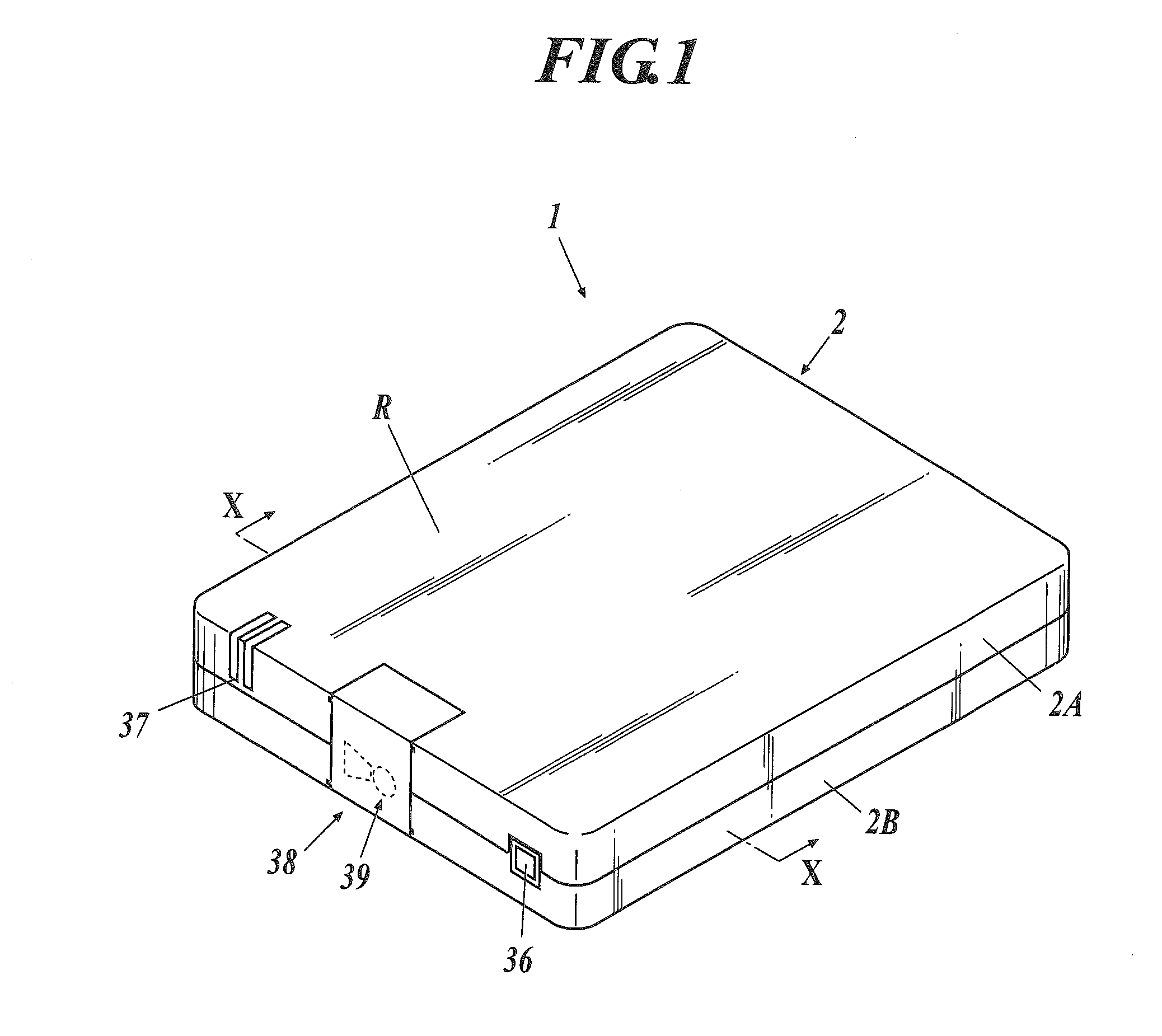
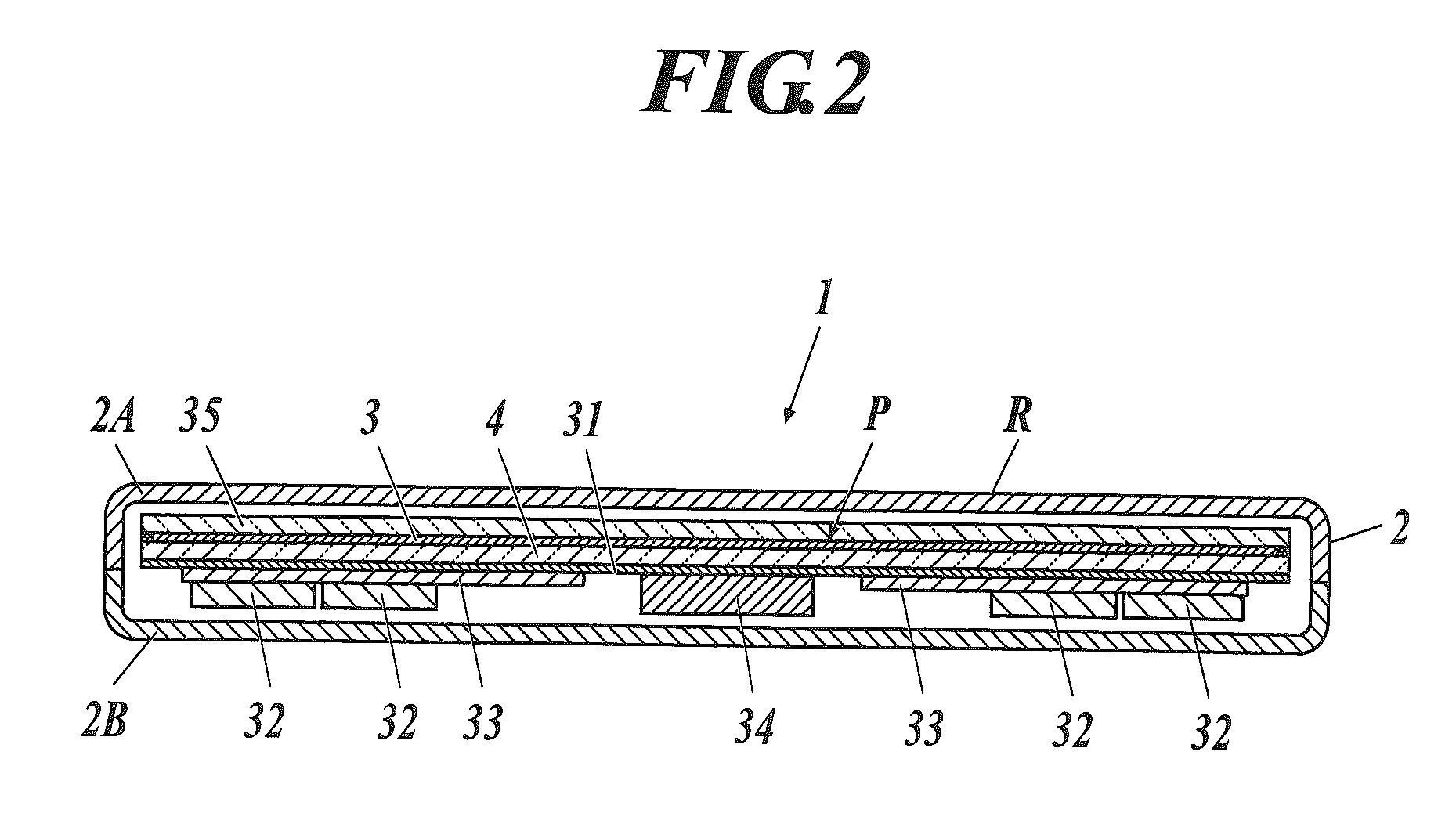
[0055]FIG. 1 is a perspective view showing the external appearance of a radiation image capturing device according to a first embodiment of the present invention. FIG. 2 is a sectional view taken along the line X-X of FIG. 1. As shown in FIGS. 1 and 2, a radiation image capturing device 1 of the embodiment is configured in such a way that a scintillator 3, a substrate 4, and the like is housed in a housing 2.
[0056]The housing 2 is made of material which radiation pass through, such as a carbon plate or plastics. At least, a radiation incidence surface R thereof is made of such material. FIGS. 1 and 2 show the housing 2 constituted of a flame plate 2A and a back plate 2B, namely, a housing in a shape of a lunch box. However, the housing 2 can be constituted of one plate to be in a shape of a rectangular cylinder, namely, a monocoque-type housing.
[0057]Furthermore, as shown in FIG. 1, a power supply switch 36, an indicator 37 constituted of an LED or the like, a cover 38 which can be ...
second embodiment
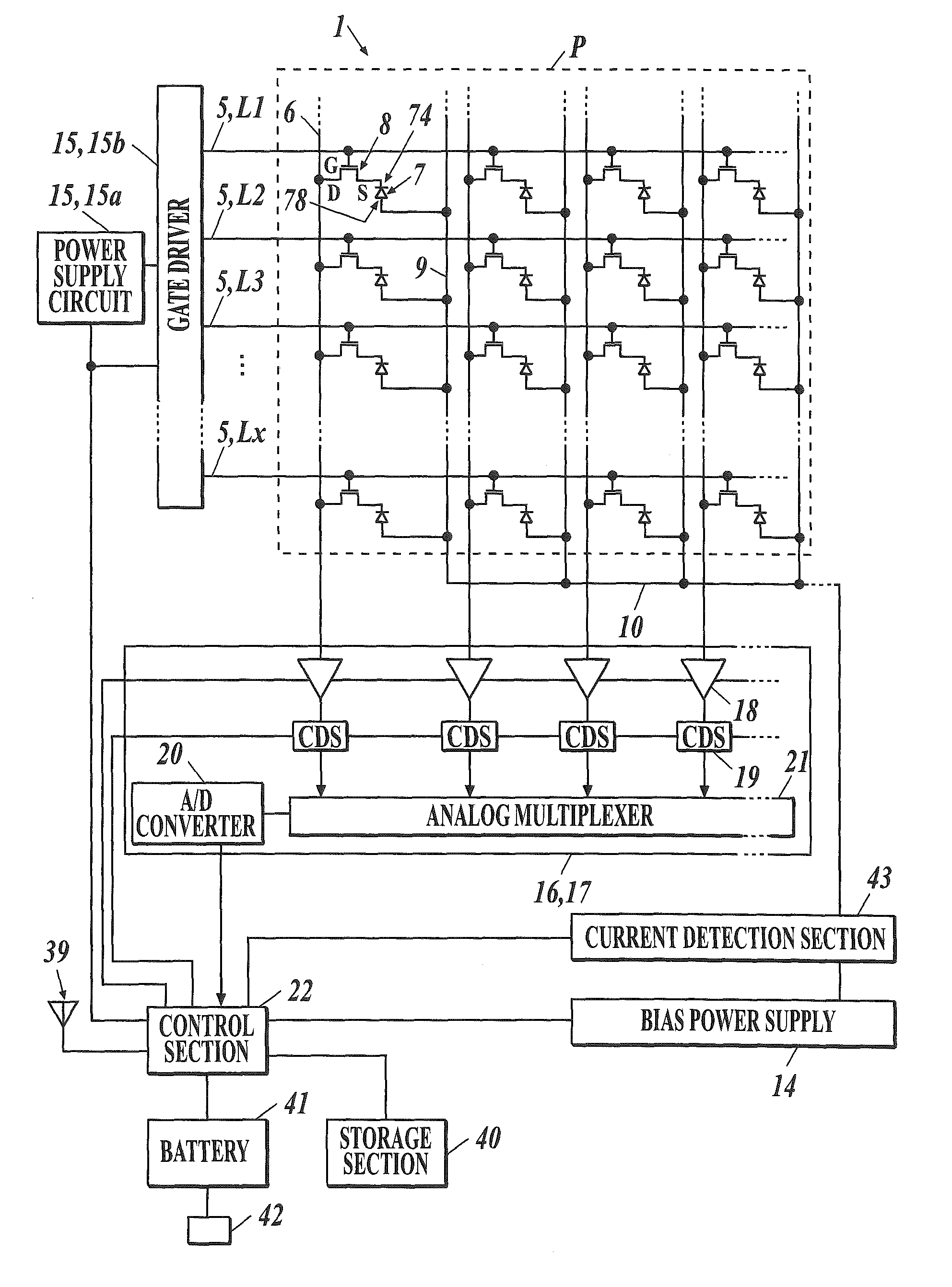
[0171]As described above, the cause of the generation of image data having a significant value in the regions R2 which are adjacent to the strongly-irradiated region R1 shown in FIG. 23A in the signal extending direction of the signal lines 6 not shown in FIGS. 23A and 23B (the up-down direction in FIG. 23B) is considered that because the electrons and the holes generated in the radiation detection elements 7 of the region R1 are discharged to the signal lines 6 and the bias lines 9, the reference potential V0 applied to the first electrodes 74 of the radiation detection elements 7 and the bias voltage Vbias applied to the second electrodes 78 thereof fluctuate.
[0172]Therefore, in the first embodiment, in the reset processing of the radiation detection elements 7 performed before the radiation image capturing, after the ON-state voltage Von1 having a predetermined voltage value is applied to the gate electrodes 8g of the TFTs 8 via the lines L1 to Lx of the scan lines 5 from the sca...
third embodiment
[0199]By the way, conventionally, in order to switch a radiation image capturing device to the charge accumulation mode, the voltage applied to the gate electrodes 8g of the TFTs 8 is switched from the ON-state voltage Von1 having a predetermined positive voltage value (shown in FIG. 11) to the OFF-state voltage Voff having a predetermined negative voltage value. However, when such a switching is carried out, a drive circuit for applying a voltage to the TFTs 8 in the gate driver 15b (shown in FIG. 7) may be overloaded, and accordingly, the drive circuit may be damaged or broken.
[0200]Furthermore, like in the first embodiment and the second embodiment, even when the ON-state voltage Von1 having a predetermined positive voltage value is applied to the gate electrodes 8g of the TFTs 8 all at once, and then the ON-state voltage Von1 is decreased all at once so that the ON-state voltage Von2 is applied thereto, there is still a possibility that the drive circuit in the gate driver 15b i...
PUM
 Abstract
Description
Claims
Application Information
 - R&D
- Intellectual Property
- Life Sciences
- Materials
- Tech Scout
- Unparalleled Data Quality
- Higher Quality Content
- 60% Fewer Hallucinations
Browse by: Latest US Patents, China's latest patents, Technical Efficacy Thesaurus, Application Domain, Technology Topic, Popular Technical Reports.
© 2025 PatSnap. All rights reserved.Legal|Privacy policy|Modern Slavery Act Transparency Statement|Sitemap|About US| Contact US: help@patsnap.com


