Semiconductor device
a technology of a semiconductor and a device body, which is applied in the direction of resonant circuit details, near-field systems using receivers, instruments, etc., can solve the problems of complex achieve the effect of simple adjustment of resonance frequency, convenient adjustment of resonance frequency and easy adjustmen
- Summary
- Abstract
- Description
- Claims
- Application Information
AI Technical Summary
Benefits of technology
Problems solved by technology
Method used
Image
Examples
embodiment 1
(Embodiment 1)
[0044]In this embodiment, an example of a semiconductor device in which the resonance frequency can be adjusted will be described.
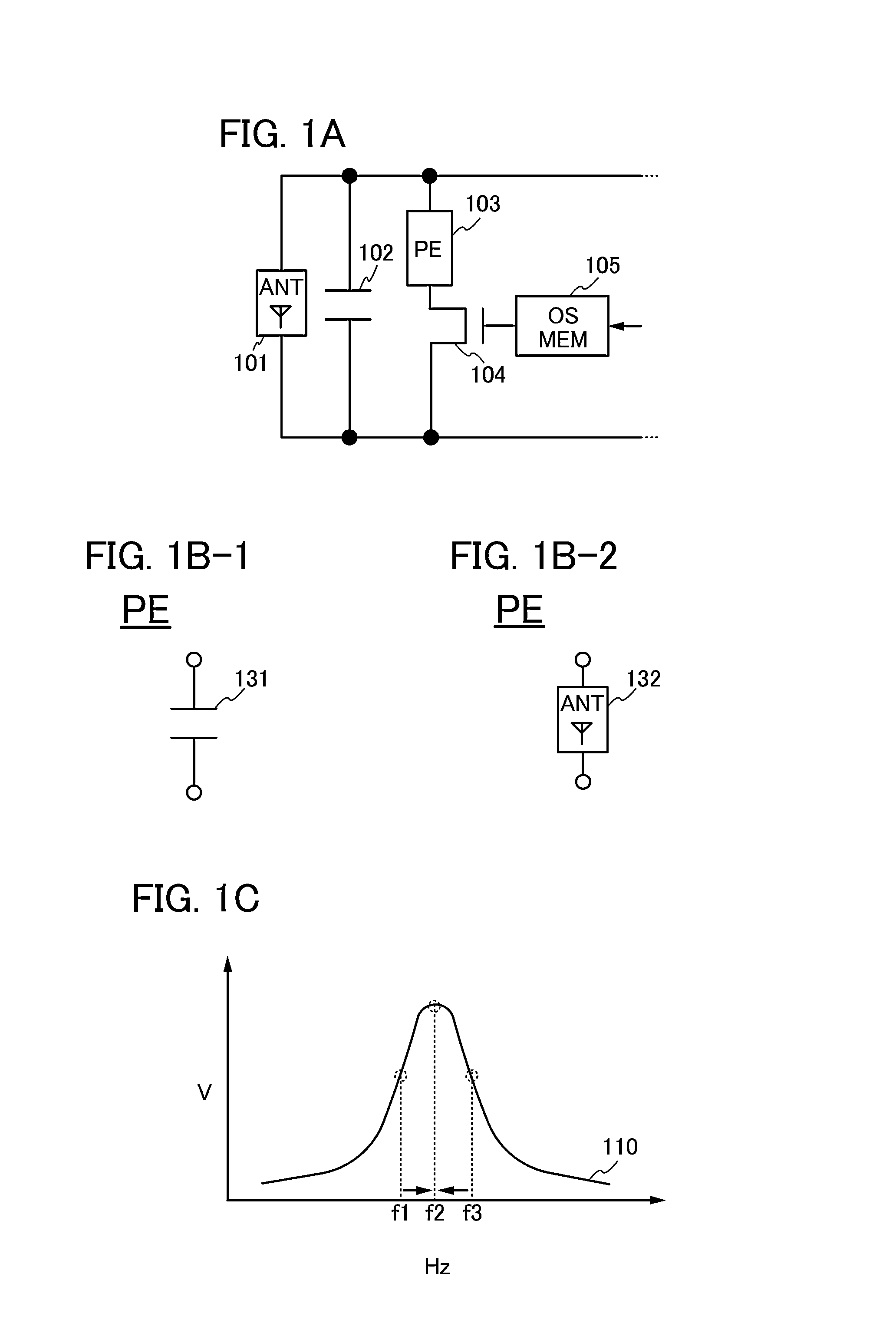
[0045]An example of the semiconductor device in this embodiment will be described with reference to FIGS. 1A, 1B-1, 1B-2, and 1C.
[0046]The semiconductor device shown in FIG. 1A includes an antenna (also referred to as ANT) 101, a capacitor 102, a passive element (also referred to as PE) 103, a transistor 104, and a memory circuit (also referred to as OSMEM) 105.
[0047]Note that the transistor includes two terminals and a current control terminal for controlling current flowing between the two terminals by voltage applied. Note that without limitation to the transistor, in an element, terminals between which current flows and the current is controlled are also referred to as current terminals. Two current terminals are also referred to as a first current terminal and a second current terminal.
[0048]A field effect transistor can be used as the ...
embodiment 2
(Embodiment 2)
[0074]In this embodiment, an example of the semiconductor device described in Embodiment 1 will be described.
[0075]An example of a semiconductor device in this embodiment will be described with reference to FIG. 3. Note that in FIG. 3, the description of the semiconductor device shown in FIG. 1A is used as appropriate for components denoted by the same reference numerals as those in the semiconductor device shown in FIG. 1A.
[0076]The semiconductor device shown in FIG. 3 includes the antenna 101, the capacitor 102, the passive element 103, the transistor 104, and the memory circuit 105, similarly to the semiconductor device shown in FIG. 1A.
[0077]The antenna 101 functions as a coil.
[0078]The capacitor 102 is electrically connected to the antenna 101 in parallel.
[0079]The passive element 103 forms a resonance circuit when electrically connected to the antenna 101 and the capacitor 102 in parallel.
[0080]The transistor 104 has a function of controlling whether the passive ...
embodiment 3
(Embodiment 3)
[0095]In this embodiment, another example of the semiconductor device described in Embodiment 1 will be described.
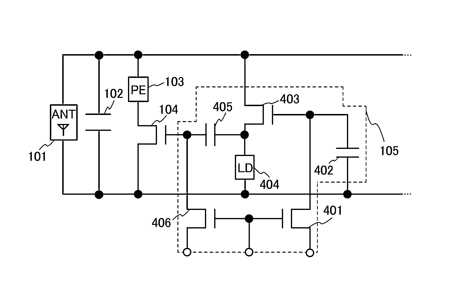
[0096]Examples of memory circuits in this embodiment will be described with reference to FIGS. 4A and 4B. FIGS. 4A and 4B are diagrams for describing the memory circuits in this embodiment. Note that in FIGS. 4A and 4B, the description of the semiconductor device shown in FIG. 1A is used as appropriate for components denoted by the same reference numerals as those in the semiconductor device shown in FIG. 1A.
[0097]Semiconductor devices shown in FIGS. 4A and 4B each include the antenna 101, the capacitor 102, the passive element 103, the transistor 104, and the memory circuit 105 similarly to the semiconductor device shown in FIG. 1A.
[0098]The antenna 101 functions as a coil.
[0099]The capacitor 102 is electrically connected to the antenna 101 in parallel.
[0100]The passive element 103 forms a resonance circuit when electrically connected to the antenna 101 an...
PUM
 Abstract
Description
Claims
Application Information
 - R&D
- Intellectual Property
- Life Sciences
- Materials
- Tech Scout
- Unparalleled Data Quality
- Higher Quality Content
- 60% Fewer Hallucinations
Browse by: Latest US Patents, China's latest patents, Technical Efficacy Thesaurus, Application Domain, Technology Topic, Popular Technical Reports.
© 2025 PatSnap. All rights reserved.Legal|Privacy policy|Modern Slavery Act Transparency Statement|Sitemap|About US| Contact US: help@patsnap.com


