
Method to transfer failure analysis-specific data between design houses and fab's/FA labs

Inactive Publication Date: 2014-02-04
DCG SYST
View PDF4 Cites 15 Cited by
  • Summary
  • Abstract
  • Description
  • Claims
  • Application Information

AI Technical Summary

Benefits of technology

The invention provides a way for an IC design house to share information about their designs with a fabrication or failure analysis facility only when the fabrication or analysis facility needs to know it. This helps the analysis facility to analyze failures more effectively without receiving unnecessary or extraneous information.

Problems solved by technology

Whereas the separation of design and fabrication tends to yield an increase in efficiency and lowering of costs, it raises some issues of concern to the manufacturers.
The transfer of information between the design houses and the fabrication companies or the failure analysis labs can cause security concerns.
In this procedure, however, the transfer of the complete design files raises security concerns, and furthermore is not essential, since the FA engineers do not require the full mask data and design information for the FA job.

Method used


Image

  • Method to transfer failure analysis-specific data between design houses and fab's/FA labs
  • Method to transfer failure analysis-specific data between design houses and fab's/FA labs
  • Method to transfer failure analysis-specific data between design houses and fab's/FA labs

Examples


Embodiment Construction

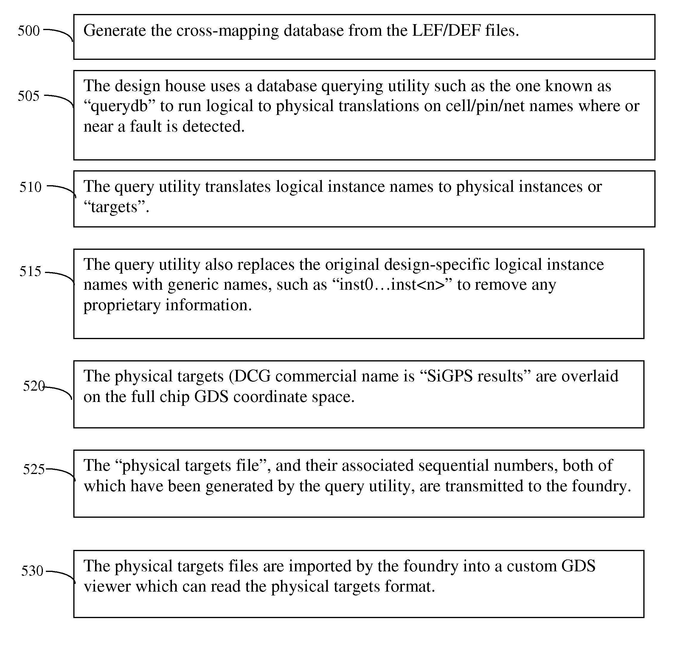
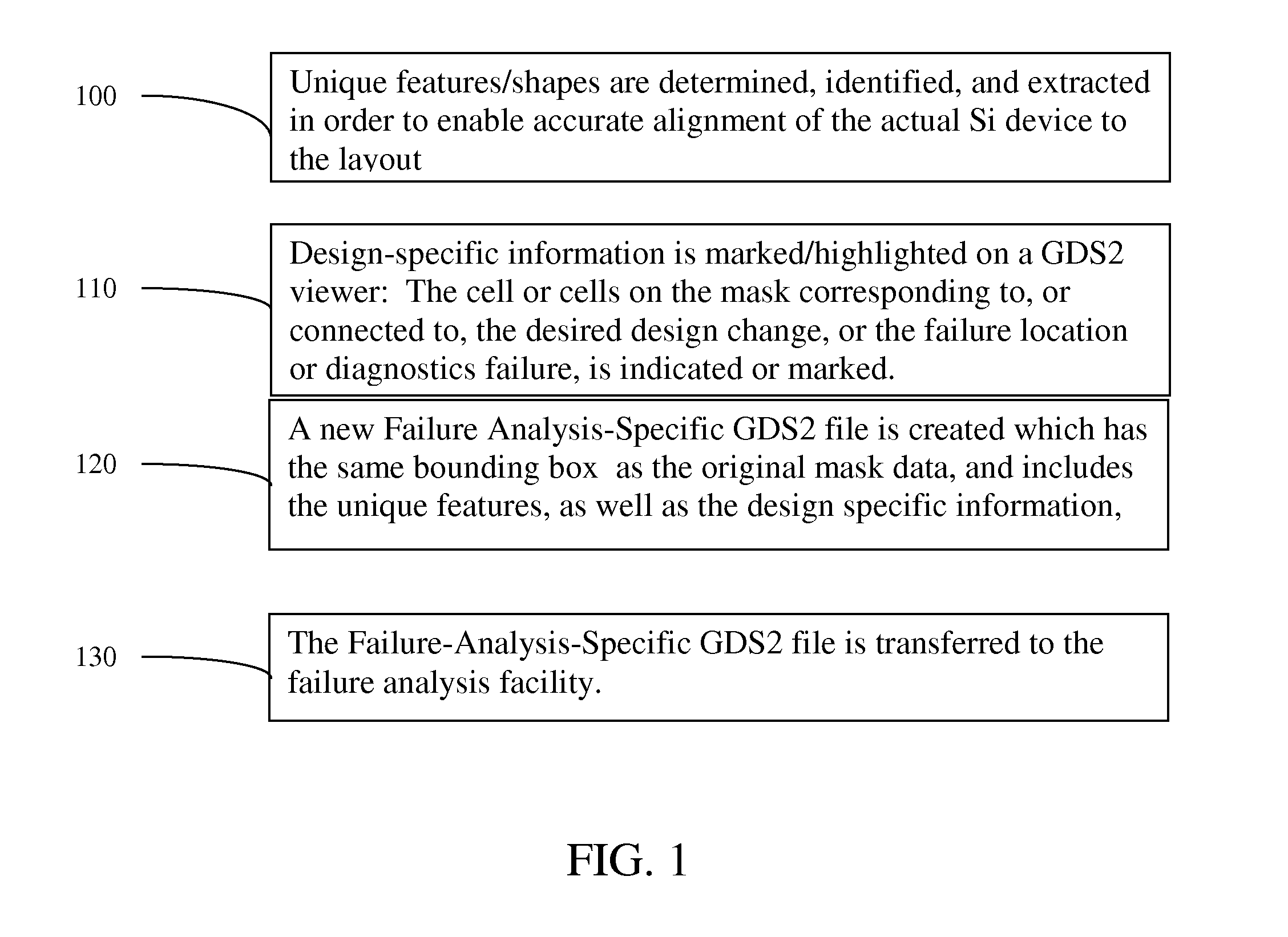
[0027]The present invention provides a method to transfer the necessary information (in addition to the standard GDS files) from the design house to the fab or facility which will be doing failure analysis on an IC, on a need-to-know basis so as to minimize security concerns. If the files are being transferred to a fab facility, the fab already has the GDS2 files, so they require the information additional to the GDS2. In case a Failure Analysis (FA) Service house is doing the analysis job, they don't need the standard GDS2 file, which is used for the fabrication. Only the necessary information, which may include some layout plus some design or connectivity information, can be extracted and sent over to them.

[0028]Failure analysis issues generally fall into three broad categories. The first is an actual failure of an operating circuit, often caused by a processing problem. A customer experiencing this type of failure will generally be able to indicate the location of the failure. Th...


PUM


Abstract

A method and system for an IC design house to transfer design and layout information to a fabrication or failure analysis facility on a need-to-know basis to enable effective failure analysis while not providing unnecessary or extraneous information.

Description

CROSS REFERENCE TO RELATED APPLICATION[0001]This application is a Continuation-in-Part of U.S. application Ser. No. 11 / 823,566 filed Jun. 28, 2007 now abandoned, and claims priority thereto. The specification of application Ser. No. 11 / 823,566 is hereby incorporated by reference in its entirety.FIELD OF THE INVENTION[0002]This invention is in the field of integrated circuit failure analysis, and more particularly in the field of transfer of design data between design houses and fab's or FA labs for failure analysis or circuit edit.BACKGROUND OF THE INVENTION[0003]In the current business environment for integrated circuit device manufacturing, an increasingly used business strategy is for the Integrated Device Manufacturers (IDM's) to go fab-lite or fab-less, and to separate the design and fabrication portions of the manufacturing by sending the fabrication portion of the jobs to dedicated fab companies such as TSMC, UMC, and Chartered.[0004]Whereas the separation of design and fabri...

Claims


Application Information

Patent Timeline
IPC IPC(8): G06F17/50
CPCG06F17/5081G06F30/398
Inventor SURI, HITESHKARDACH, CATHARINE L.
Owner DCG SYST
Learn More