Liquid crystal display including subpixel electrodes having fine protruding patterns
a liquid crystal display and subpixel electrode technology, applied in non-linear optics, instruments, optics, etc., can solve the problems of unstable directionality of liquid crystals, difficult to effectively control liquid crystals, poor lateral visibility, etc., to reduce the response time of liquid crystals, improve the light transmission of each pixel, and increase the effective aperture ratio of each pixel
- Summary
- Abstract
- Description
- Claims
- Application Information
AI Technical Summary
Benefits of technology
Problems solved by technology
Method used
Image
Examples
first embodiment
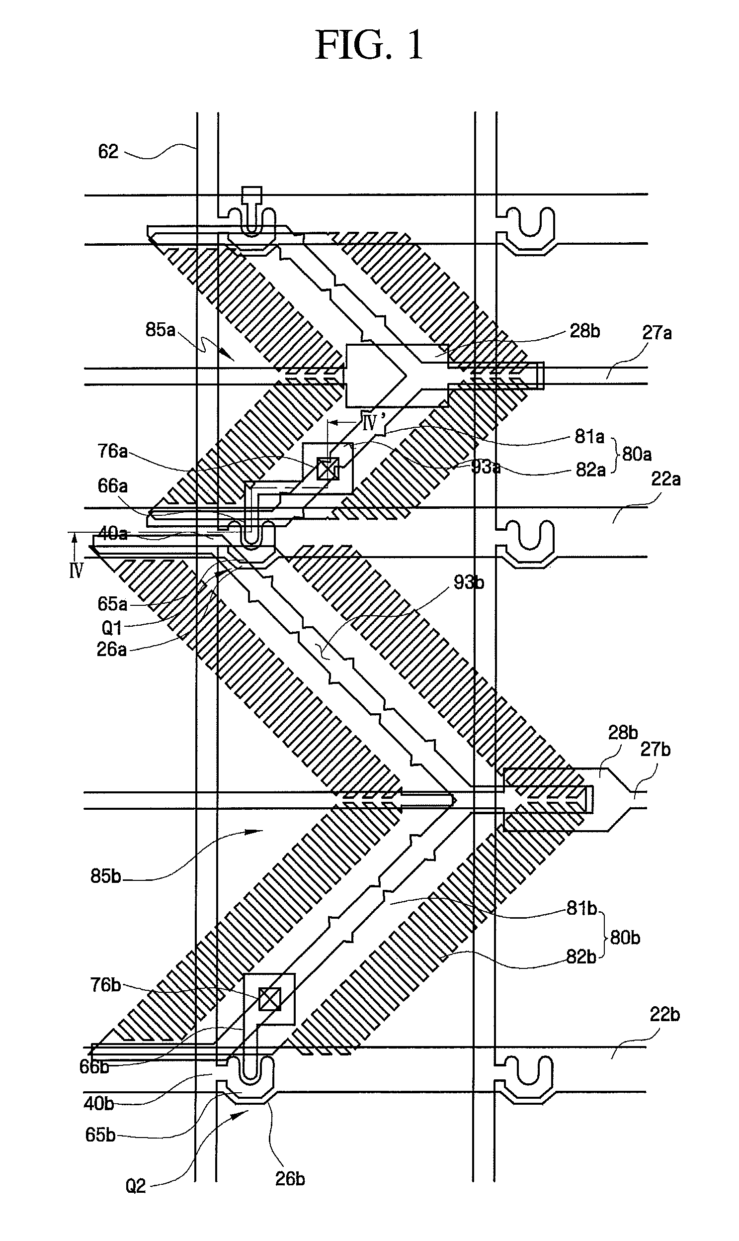
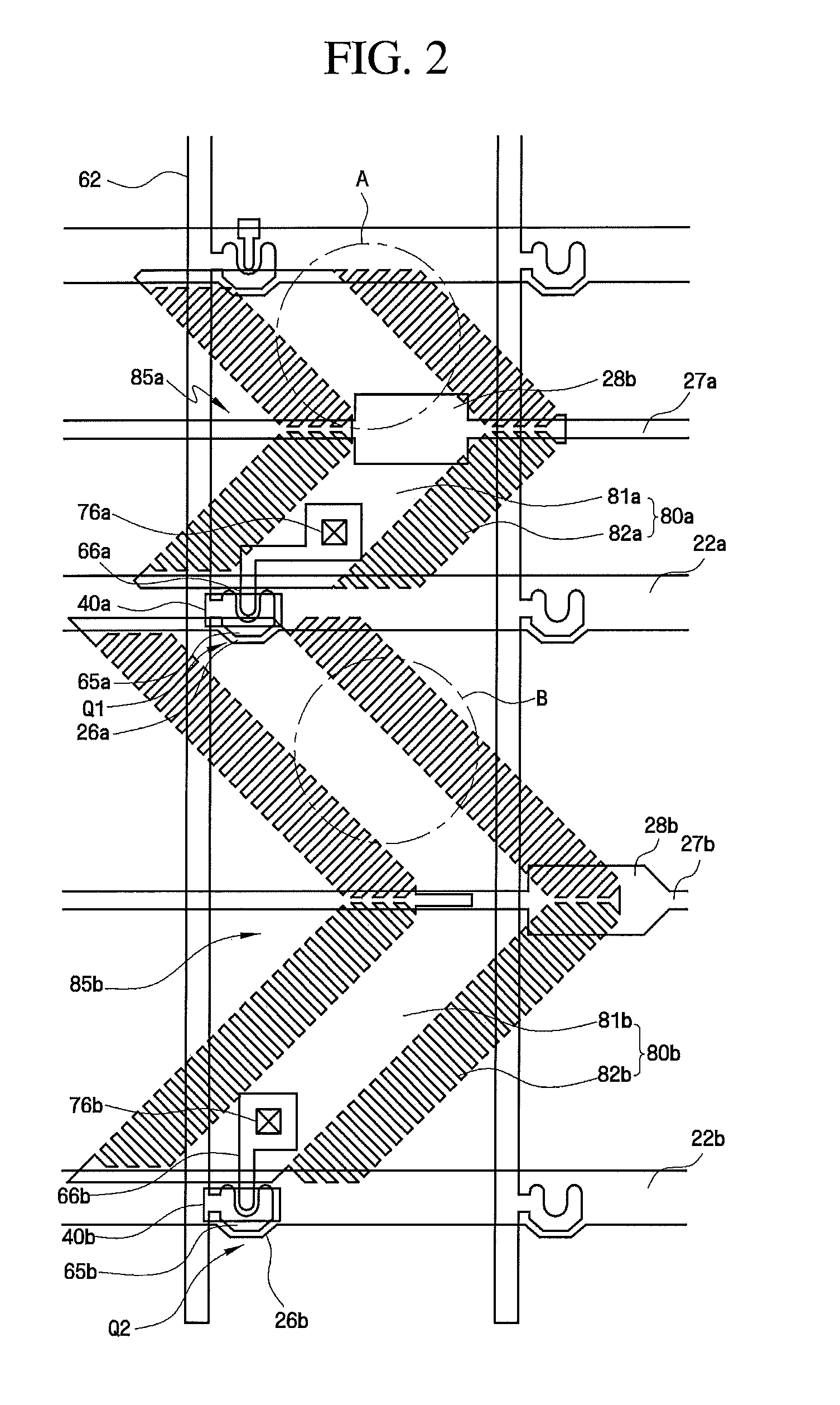
[0028]Hereinafter, a liquid crystal display (LCD) according to one embodiment will be described in detail with reference to FIGS. 1 through 6B. FIG. 1 is an arrangement plan of the LCD according to the present invention. FIG. 2 is an arrangement plan of a thin-film transistor (TFT) display plate 100 of the LCD shown in FIG. 1. FIG. 3 is an arrangement plan of a common electrode display plate 200 of the LCD shown in FIG. 1. FIG. 4 is a cross-sectional view of the LCD taken along a line IV-IV′ of FIG. 1.
[0029]Referring to FIGS. 1 through 4, the LCD according to the first embodiment includes a TFT display plate 100, a common electrode display plate 200 facing the TFT display plate 100, and a liquid crystal layer 300 interposed between the TFT display plate 100 and the common electrode display plate 200.
[0030]First and second gate lines 22a and 22b are formed on a first insulating substrate 10 which is made of transparent glass. The first and second gate lines 22a and 22b generally exte...
second embodiment
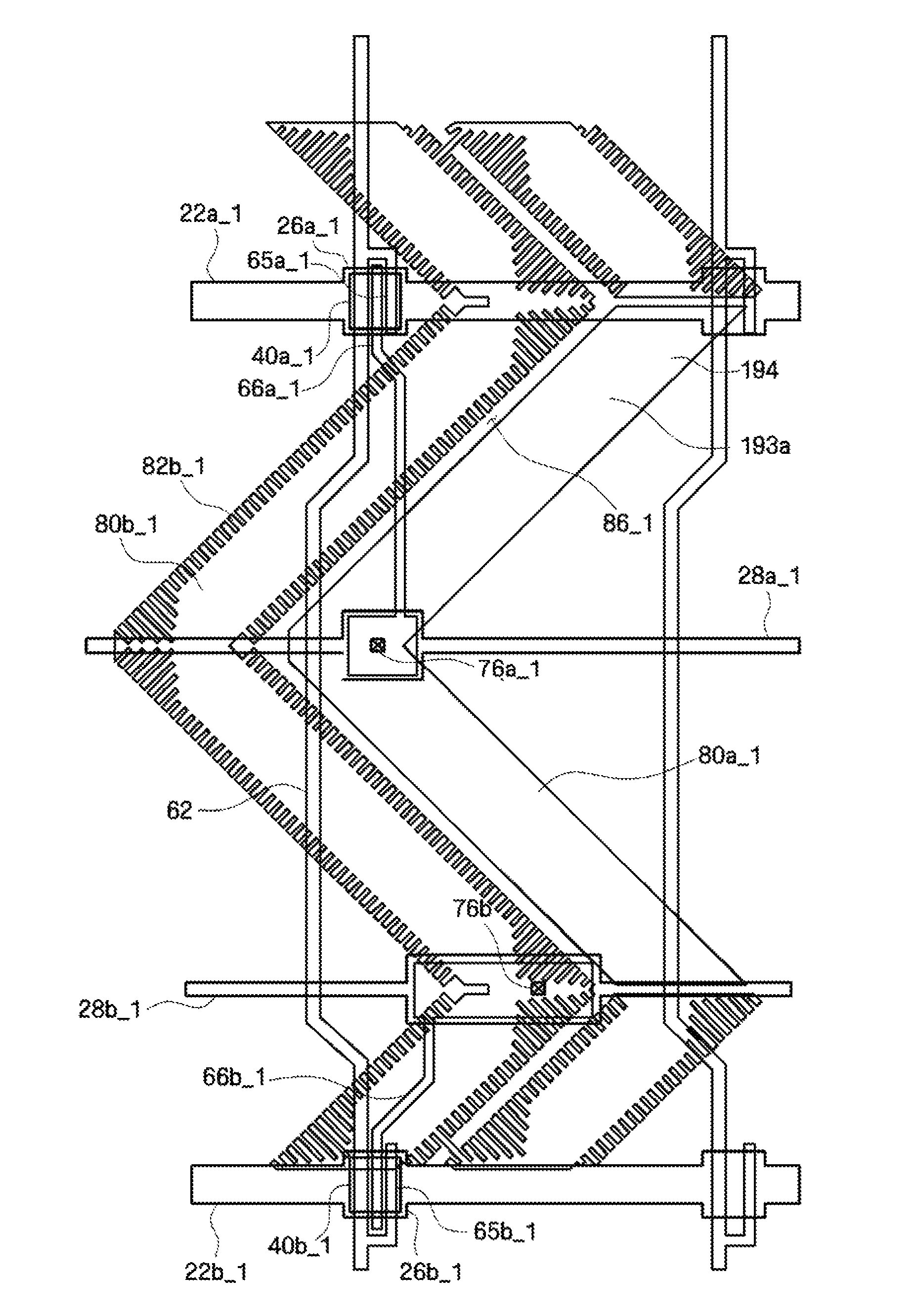
[0069]Referring to FIGS. 7 through 9, the LCD includes a first subpixel electrode 80a_1, which does not have fine patterns; a second subpixel electrode 80b_1, which has fine patterns; and a common electrode 191 which has fine patterns at a location corresponding to the first subpixel electrode 80a_1.
[0070]The TFT display plate includes first and second gate lines 22a_1 and 22b_1 formed on a first insulating substrate 10. The first and second gate lines 22a_1 and 22b_1 extend horizontally and parallel to each other. The TFT display plate also includes a data line 62_1 which crosses the first and second gate lines 22a_1 and 22b_1. The first and second gate lines 22a_1 and 22b_1 have first and second gate electrodes 26a_1 and 26b_1, respectively.
[0071]First and second subpixel electrodes 80a_1 and 80b_1 may be bent in a zigzag manner and may be separated from each other by a slit 86_1 which is a domain formation portion. However, the domain formation portion may not be limited to the ...
third embodiment
[0075]Referring to FIG. 10, the LCD includes a first subpixel electrode 80a_2 having a plurality of first fine protruding patterns 82a_2 separated from each other by a first gap 83a_2, and a second subpixel electrode 80b_2 having a plurality of second fine protruding patterns 82b_1 separated from each other by a second gap 83b_2. A length of each of the first fine protruding patterns 82a_1 may be greater than that of each of the second fine protruding patterns 82b_1. In addition, the sum of a width of each of the first fine protruding patterns 82a_1 and a width of the first gap 83a_1 may be greater than the sum of a width of each of the second fine protruding patterns 82b_2 and a width of the second gap 83b_2.
[0076]The first and second subpixel electrodes 80a_2 and 80b_2 may be bent in a zigzag manner and may be separated from each other by a slit 86_2 which is a domain formation portion.
[0077]The first subpixel electrode 80a_2 includes a first flat portion 81a_2 in the middle ther...
PUM
| Property | Measurement | Unit |
|---|---|---|
| data voltage | aaaaa | aaaaa |
| area | aaaaa | aaaaa |
| length | aaaaa | aaaaa |
Abstract
Description
Claims
Application Information
 - R&D
- Intellectual Property
- Life Sciences
- Materials
- Tech Scout
- Unparalleled Data Quality
- Higher Quality Content
- 60% Fewer Hallucinations
Browse by: Latest US Patents, China's latest patents, Technical Efficacy Thesaurus, Application Domain, Technology Topic, Popular Technical Reports.
© 2025 PatSnap. All rights reserved.Legal|Privacy policy|Modern Slavery Act Transparency Statement|Sitemap|About US| Contact US: help@patsnap.com


