Substrate supports for semiconductor applications
a technology for semiconductor applications and substrates, applied in the direction of liquid surface applicators, coatings, electrical devices, etc., can solve the problems of reducing or losing attractive force, affecting the attractive force of dislodged substrates, so as to reduce current leakage, enhance the attractive or chucking force, and eliminate the concern of electrostatic attraction force varying
- Summary
- Abstract
- Description
- Claims
- Application Information
AI Technical Summary
Benefits of technology
Problems solved by technology
Method used
Image
Examples
example 1
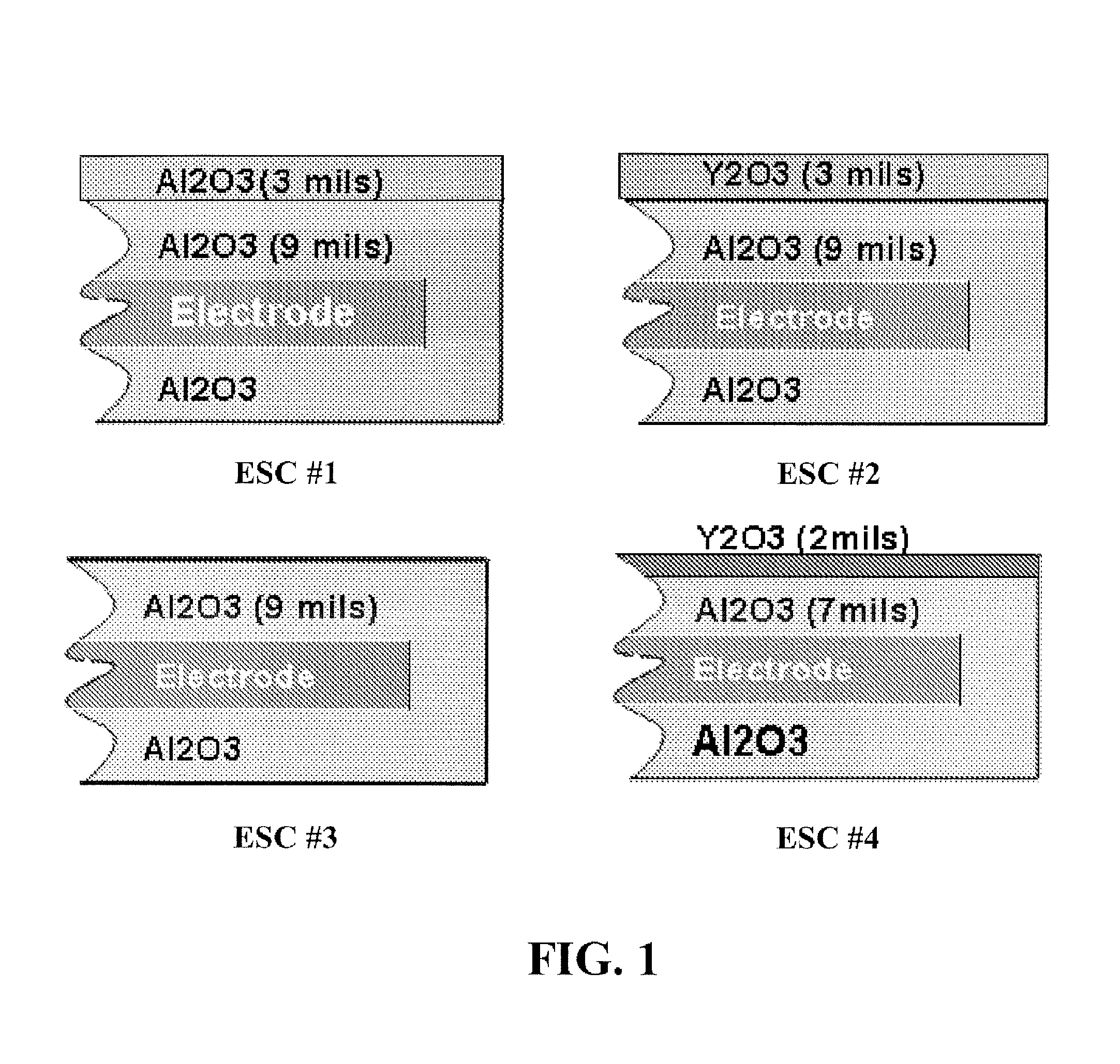
[0072]Four different electrostatic chucks (ESCs) for a 300 mm wafer were fabricated to compare chucking force. The four ESCs are shown in cross section in FIG. 1. ESC #1 and ESC#2 were one test set and ESC #3 and ESC#4 were another test set. ESC #1 was coated with an Al2O3 undercoat layer (9 mils) and an Al2O3 topcoat layer (3 mils). ESC #2 was coated with an Al2O3 undercoat layer (9 mils) and a Y2O3 topcoat layer (3 mils). ESC #3 was coated with a single Al2O3 layer (9 mils). ESC #4 was coated with an Al2O3 undercoat layer (7 mils) and a Y2O3 topcoat layer (2 mils).
[0073]In order to make sure that the factors affecting on chucking force such as surface roughness of the ESC surface contacting the wafer and contact ratio with the wafer, the resistance of each layer and thickness were checked before the chucking force was measured.
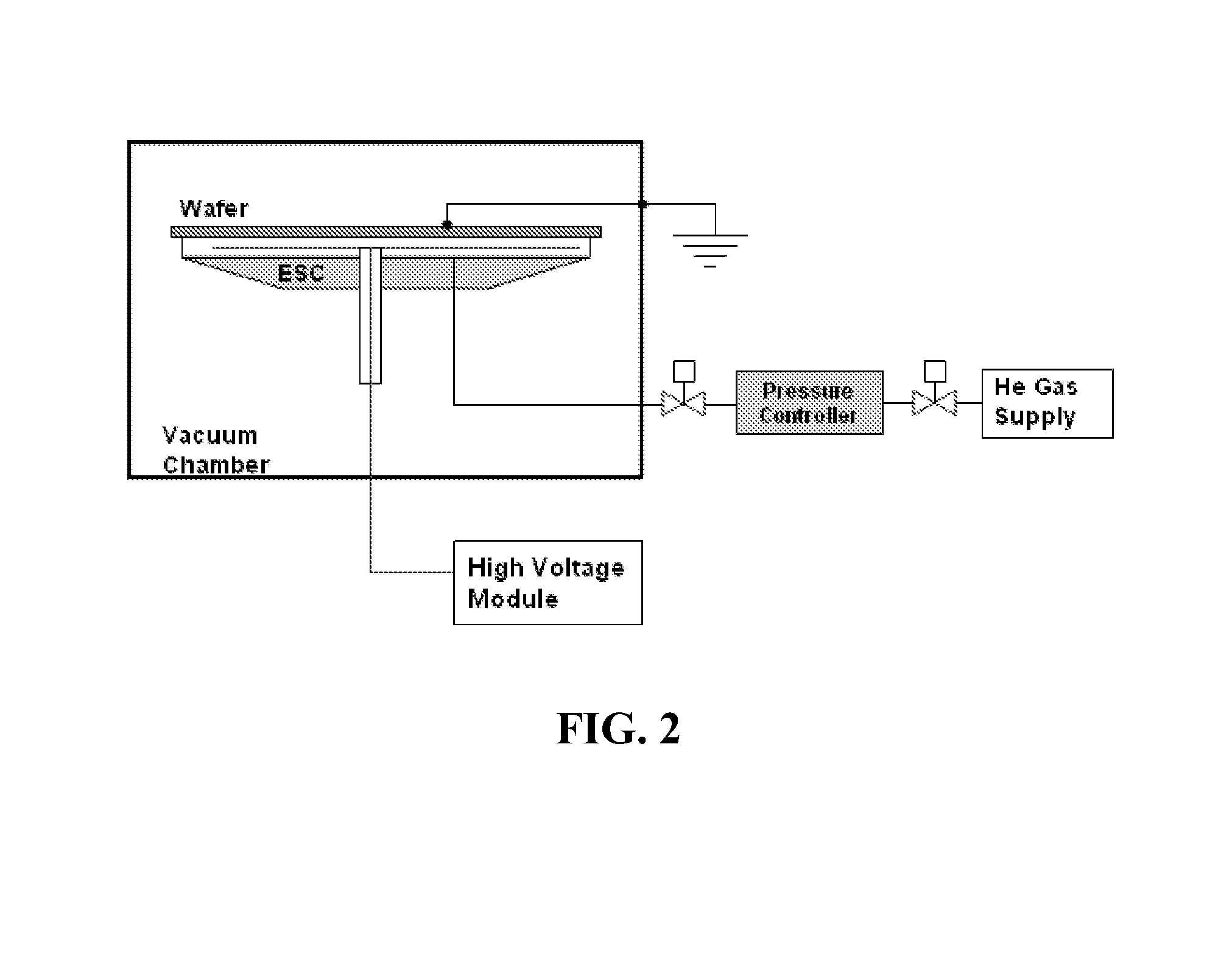
[0074]In order to measure the chucking force, gas was introduced in between the wafer and each ESC and the flow rate of the gas leaking through the peripher...
example 2
[0086]Plasma resistance was determined for the yttria topcoat layer. The measurement technique utilized to obtain this data was very precise, i.e., + / −0.5 micrometers. A Zeiss Confocal microscope (CSM 700) was used to measure the step height. Coating surfaces were polished to very smooth finishes (i.e., about 7 microns) in order to ensure the step height due to plasma erosion could clearly be differentiated. The number of measurements per sample and the number of replicates are provided in FIG. 4. The magnitudes measured were after 60 total hours of exposure. The data shows that yttria erodes about 2-3 micrometers after 60 hours of exposure with CF4 / O2 reactive ion etching (RIE). In comparison, the data shows that alumina erodes about 16 micrometers after 60 hours with CF4 / O2 RIE. This amounts to an erosion rate of about 5-8× greater for alumina as compared to yttria.
example 3
[0087]Al2O3 is typically used for parts exposed to plasma in a plasma process chamber. The reaction of Al2O3 with gases including fluorine (e.g., NF4 or CF4 to be used for cleaning in a deposition process and etchant in an etch process) produces AlF on the Al2O3 surface. This causes a particle issue resulting in changes in material properties and process drift with time. In accordance with this invention, a Y2O3 coating on top of Al2O3 can be used as the dielectric material for an ESC. A Y2O3 coating on top of Al2O3 is also desirable because Y2O3 does not react with fluorine.
PUM
| Property | Measurement | Unit |
|---|---|---|
| dielectric constant | aaaaa | aaaaa |
| thickness | aaaaa | aaaaa |
| thickness | aaaaa | aaaaa |
Abstract
Description
Claims
Application Information
 - R&D
- Intellectual Property
- Life Sciences
- Materials
- Tech Scout
- Unparalleled Data Quality
- Higher Quality Content
- 60% Fewer Hallucinations
Browse by: Latest US Patents, China's latest patents, Technical Efficacy Thesaurus, Application Domain, Technology Topic, Popular Technical Reports.
© 2025 PatSnap. All rights reserved.Legal|Privacy policy|Modern Slavery Act Transparency Statement|Sitemap|About US| Contact US: help@patsnap.com


