Display device and method of manufacturing the same

a technology of display device and manufacturing method, which is applied in the direction of semiconductor devices, basic electric elements, electrical apparatus, etc., can solve the problems of increased process cost and difficulty in incorporating low resistance wires, and achieve the effect of increasing process cost and low resistance wires

Active Publication Date: 2013-08-20
SAMSUNG DISPLAY CO LTD
View PDF12 Cites 0 Cited by
  • Summary
  • Abstract
  • Description
  • Claims
  • Application Information

AI Technical Summary

Benefits of technology

[0009]Aspects of the described technology have been made in an effort to provide a display device and a method of manufacturing the same having advantages of embodying a low resistance wire without increasing process cost.
[0022]A display device according to aspects of the present invention can reduce the process cost by reducing the number of mask processes while embodying a low resistance wire.

Problems solved by technology

However, because resistance of a wire increases by a heat treatment process for crystallization or activation in an existing low-temperature poly-Si (LTPS) process or heat crystallization process, it is difficult to embody a low resistance wire, and when further using a mask in order to avoid such a problem, there is a problem that process cost increases.

Method used


Image

  • Display device and method of manufacturing the same
  • Display device and method of manufacturing the same
  • Display device and method of manufacturing the same

Examples


Embodiment Construction

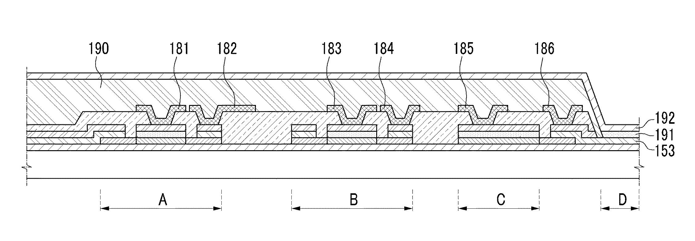
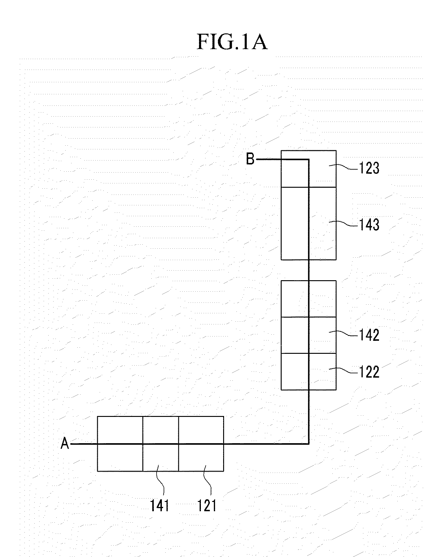
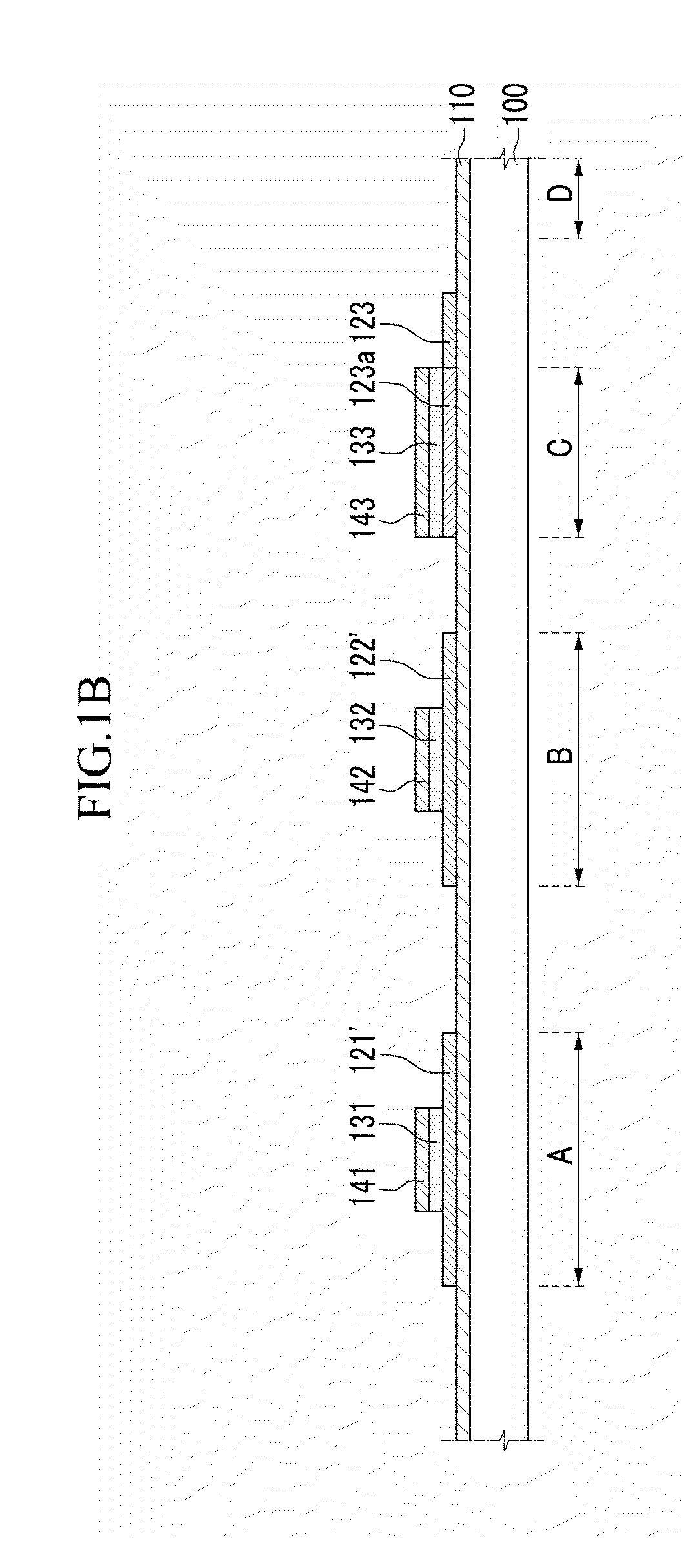
[0028]Reference will now be made in detail to the present embodiments of the present invention, examples of which are illustrated in the accompanying drawings, wherein like reference numerals refer to the like elements throughout. The embodiments are described below in order to explain the present invention by referring to the figures. Moreover, it is to be understood that where it is stated herein that one layer is “formed on” or “disposed on” a second layer, the first layer may be formed or disposed directly on the second layer or there may be an intervening layer between the first layer and the second layer. Further, as used herein, the terms “formed on” and the like may be used with the same meaning as “located on” or “disposed on” and are not meant to be limiting regarding any particular fabrication process.

[0029]Further, in the exemplary embodiments, like reference numerals designate like constituent elements having the same configuration. Otherwise, configurations different a...


PUM


Abstract

A display device with the substrate divided into three areas. A semiconductor layer is formed in the first second areas and includes a channel area and source / drain areas; a gate insulating layer formed on the semiconductor layer in an area corresponding to the channel area; and a gate electrode formed on the gate insulating layer. The source / drain electrodes contact the source / drain areas, respectively; a pixel electrode is formed in the same layer but in a third area; an interlayer insulating layer is formed on a whole surface of the substrate including the formed structures; and a gate line is formed on the interlayer insulating layer and is electrically connected to a gate electrode of the first area through a via contact hole of the interlayer insulating layer.

Description

CROSS-REFERENCE TO RELATED APPLICATION[0001]This application claims the benefit of Korean Application No. 10-2010-0049334, filed May 26, 2010 in the Korean Intellectual Property Office, the disclosure of which is incorporated herein by reference.BACKGROUND[0002]1. Field[0003]Aspects of the described technology relate generally to a display device and a method of manufacturing the same. More particularly, aspects of the described technology relate generally to a display device embodying a low resistance wire.[0004]2. Description of the Related Art[0005]In general, an organic light emitting diode (OLED) display, which is one of the types of display devices, is a self luminescent display that emits light by electrically exciting a fluorescent organic compound. The OLED displays are divided into a passive matrix method and an active matrix method according to a method of driving the pixels that are disposed in a matrix form. An active matrix organic light emitting diode (AMOLED) element...

Claims


Application Information

Patent Timeline
Patent Type & Authority Patents(United States)
IPC IPC(8): H01L27/14
CPCH01L27/3279H01L27/3248H10K59/123H10K59/1315H01L27/124
Inventor SHIN, MIN-CHULCHO, KYU-SIKLEE, WON-KYUYANG, TAE-HOONCHOO, BYOUNG-KWONLEE, YUN-GYUPARK, YONG-HWANMOON, SANG-HOCHOI, BO-KYUNG
Owner SAMSUNG DISPLAY CO LTD
Why Eureka
Try Eureka