
Gate driving circuit for power semiconductor element

a driving circuit and semiconductor technology, applied in the direction of pulse generators, emergency protective arrangements for limiting excess voltage/current, pulse techniques, etc., can solve the problems of hard interruption of igbt b>1/b>, rapid decrease of voltage vg, and noise generation of igbt b>1/b>, so as to avoid device breakdown and suppress noise generation

Active Publication Date: 2013-06-18
FUJI ELECTRIC CO LTD
View PDF10 Cites 9 Cited by
  • Summary
  • Abstract
  • Description
  • Claims
  • Application Information

AI Technical Summary

Benefits of technology

[0024]It is therefore an object of the present invention to solve the problems and provide a gate driving circuit for a power semiconductor element that quickly and surely performs soft interruption of the element in the event of overcurrent and short circuit, thereby avoiding device breakdown and suppressing noise generation.
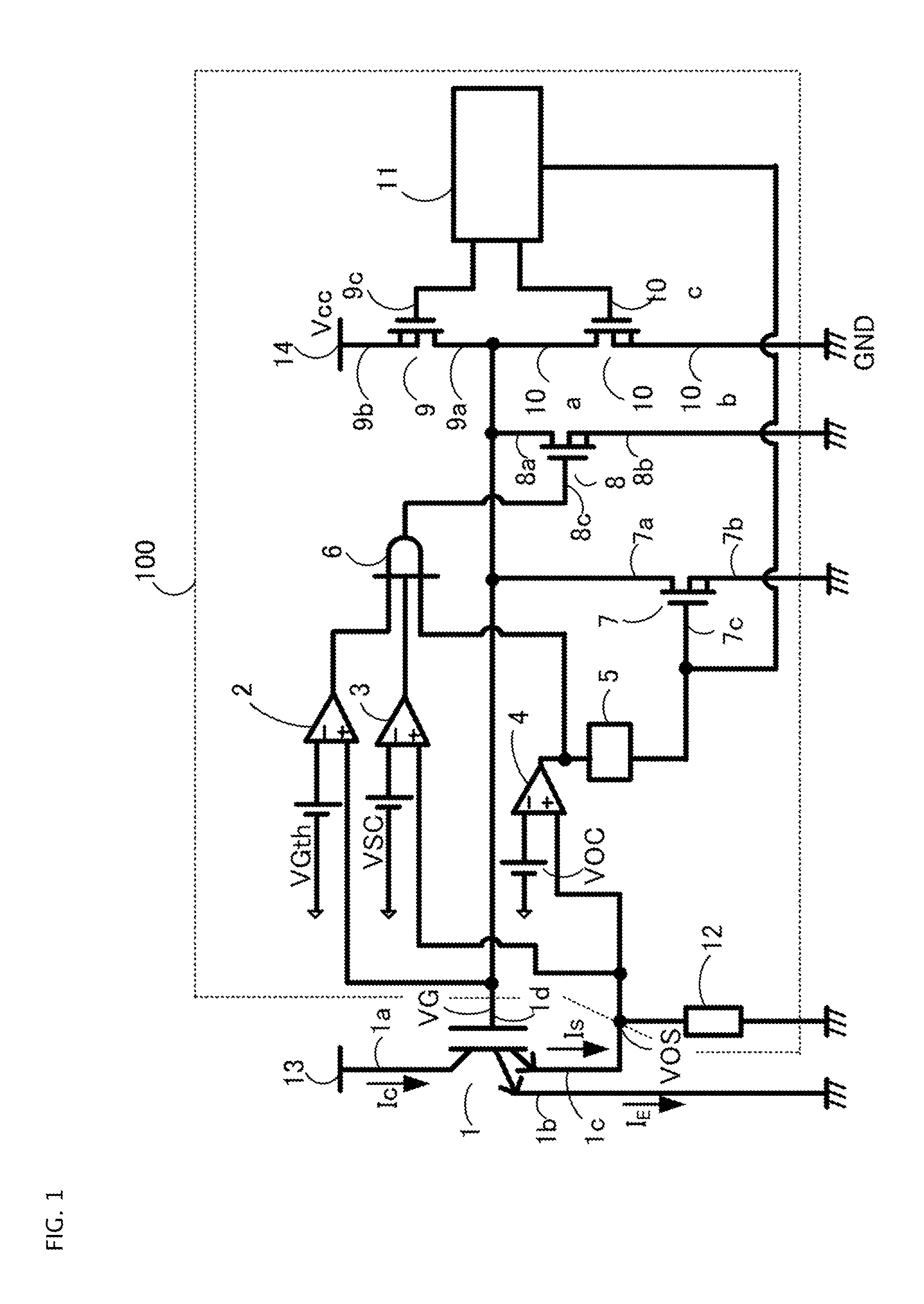
[0033]A gate driving circuit according to the present invention comprises a switching element for rapidly drawing out the charges accumulated on the gate of a power semiconductor element and a switching element for slowly drawing out the charges. By turning the switching elements ON at different times, soft interruption of the element is performed rapidly and surely on an event of overcurrent or short circuit current. Therefore, device breakdown is avoided and generation of noises is suppressed.

Problems solved by technology

As a result, the gate voltage VG rapidly decreases and the collector current IC rapidly decreases as well, causing hard interruption of the IGBT 1.
The hard interruption of the IGBT 1 makes noises and thus, undesirable.
In the case of load short circuit or large gate capacitance of the IGBT in this construction, a long time is necessary to draw out the charges on the gate due to the effect of a mirror capacitance.
During that period, over current or short circuit current continues to flow in the IGBT 1, resulting in breakdown of the element.
However, the documents are silent about a gate driving circuit for suppressing accompanied noise generation.

Method used


Image

  • Gate driving circuit for power semiconductor element
  • Gate driving circuit for power semiconductor element
  • Gate driving circuit for power semiconductor element

Examples


example 1

[0048]FIG. 1 is a circuit diagram of an essential part of a gate driving circuit for a power semiconductor element of a first embodiment according to the invention. A power semiconductor element is an IGBT 1 in this embodiment example. The IGBT 1 has a sense emitter 1c for detecting the main current, which is a collector current Ic. The region encircled by the dotted lines in FIG. 1 is the gate driving circuit 100.

[0049]A collector 1a of the IGBT 1 is connected to a high potential side 13 of a main power supply, and an emitter 1b is connected to the GND, which is a low potential side of the main power supply. A sense emitter is connected to the GND through a sense resistor 12. An emitter current IE is the main current flowing in the emitter 1b. VOS is a voltage generated by a sense current Is flowing through the sense resistor 12 to the GND. The collector current Ic in the IGBT 1 is divided into the emitter current IE and the sense current Is. The magnitude of the sense current Is i...

example 2

[0073]FIG. 3 is a circuit diagram of an essential part of a gate driving circuit for a power semiconductor element of Example 2 according to the present invention.

[0074]This gate driving circuit 200 is different from the gate driving circuit 100 in that a one-shot circuit 15 is additionally provided in the gate driving circuit 200. The S terminal of the one-shot circuit 15 is connected to the output terminal of the logic circuit 6; the R terminal is connected to the output terminal of the gate voltage monitoring circuit 2; and the Q terminal is connected to the gate 8c of the MSINK 8. The one-shot circuit 15 is composed of a flip-flop circuit that performs a set function and a reset function.

[0075]Owing to provision of the one-shot circuit 15, the gate driving circuit 200 allows fast falling down of the gate voltage VG as in the Example 1 even in the case accompanying oscillation of a short circuit current.

[0076]Operation waveforms of the gate driving circuit 200 are as same as thos...

example 3

[0078]FIG. 4 is a circuit diagram of an essential part of a gate driving circuit for a power semiconductor element of Example 3 according to the present invention.

[0079]This gate driving circuit 300 is different from the gate driving circuit 100 of FIG. 1 in that a second MSINK 16 is provided in addition to the one-shot circuit 15 in FIG. 3. Since the charges on the gate 1d of the IGBT 1 are drawn out also through the second MSINK 16, the gate voltage VG decreases faster than the one in the gate driving circuit 100 of FIG. 1 and the collector current Ic becomes into a decreasing process earlier. Consequently, device breakdown due to overcurrent or short circuit is more surely avoided.

[0080]Falling down of the gate voltage VG does not delay even in the case accompanying oscillation in short circuit current as in the gate driving circuit 200 of FIG. 3.

[0081]FIG. 5 shows operation waveforms in the gate driving circuit 300 of FIG. 4. The dotted lines in FIG. 5 show the waveforms in FIG....


PUM


Abstract

A gate driving circuit for driving a power semiconductor element can include a MSINK that is an n-channel metal-oxide silicon field-effect transistor (MOSFET) with a low resistance value for rapidly drawing out the charges accumulated on the gate of an insulated gate bipolar transistor (IGBT), and a MSOFT that is an n-channel MOSFET with a high resistance value for slowly drawing out the charges. By shifting the time for turning ON of these MOSFETs, soft interruption can be performed rapidly and surely when overcurrent or short circuit current flows in the IGBT. Therefore, device breakdown is minimized or avoided and noise generation is suppressed.

Description

BACKGROUND OF THE INVENTION[0001]1. Field of the Invention[0002]Embodiments of the invention relate to a gate driving circuit for a power semiconductor element, and, in particular, to a gate driving circuit implementing an overcurrent protection circuit and a short circuit protection circuit.[0003]2. Description of the Related Art[0004]An intelligent power module (hereinafter referred to as an “IPM”) is known as a semiconductor device used in a power conversion apparatus such as an inverter or a chopper. An IPM includes a plurality of semiconductor chips such as IGBT chips, and a driving circuit and a protection circuit therefor contained in a single package.[0005]FIG. 9 is a circuit diagram of a conventional gate driving circuit 700 for an IGBT. The gate driving circuit is the part encircled by the dotted lines. A collector 1a of the IGBT 1 is connected to a main power supply not depicted in the figure. An emitter 1b of the IGBT 1 is connected to the GND, and a sense emitter is con...

Claims


Application Information

Patent Timeline
Patent Type & Authority Patents(United States)
IPC IPC(8): H03K17/30
CPCH03K17/0828
Inventor MORI, TAKAHIRO
Owner FUJI ELECTRIC CO LTD
Learn More