Printed circuit board connector

a technology of printed circuit board and connector, which is applied in the direction of coupling device connection, coupling/disconnecting parts engagement/disengagement, electrical apparatus, etc., can solve the problems of reduced space for mounting other electronic components, inability to ensure co-planarity of solder joint surfaces of the plurality of lead portions, and , so as to improve the mounting quality and uniform solder bonding thickness.

Active Publication Date: 2013-06-18
JST MFG CO LTD
View PDF6 Cites 1 Cited by
  • Summary
  • Abstract
  • Description
  • Claims
  • Application Information

AI Technical Summary

Benefits of technology

[0014]An object of the present invention is to provide a printed circuit board connector wherein solder-bonded surfaces of lead portions of contacts arranged in parallel in a longitudinal direction of the housing contact the printed circuit board uniformly, and that improves connector mounting quality by making a uniform solder bonding thickness.
[0024]The printed circuit board connector according to the embodiment of the present invention is structured to hold a plurality of contacts having lead portions solder-bonded to the printed circuit board to be able to swing in only one direction on the printed circuit board. For that reason, the plurality of lead portion solder-bonding surfaces is solder-bonded along warping or twisting that occurs. They are able to absorb manufacturing error caused by warping or torsion of the housing or printed circuit board. Furthermore, it is possible to reduce the effects on lead portion solder-bonding strength. Specifically, mounting quality of the connector is improved.

Problems solved by technology

However, in a plan view, this kind of reinforcing tab extends outward from the connector shell occupying a certain amount installation space on the printed circuit board.
This causes a problem of reduced space for mounting other electronic components.
However, because the housing 7 is formed from plastic, thermal strain can causes warping in a length direction of the back-wall portion 71.
For that reason, there is a problem that co-planarity cannot be ensured for the solder joint surfaces of the plurality of lead portions 9b.
Therefore, while the plurality of lead portions 9b may be in contact with the printed circuit board surface at both end portions, for example, there is a problem in that the lead portions 9b may become slightly separated from the printed circuit board surface at a central portion if warping occurs, for example.
This makes it difficult to obtain a uniform solder thickness.

Method used


Image

  • Printed circuit board connector
  • Printed circuit board connector
  • Printed circuit board connector

Examples


first embodiment

Printed Circuit Board Connector Configuration

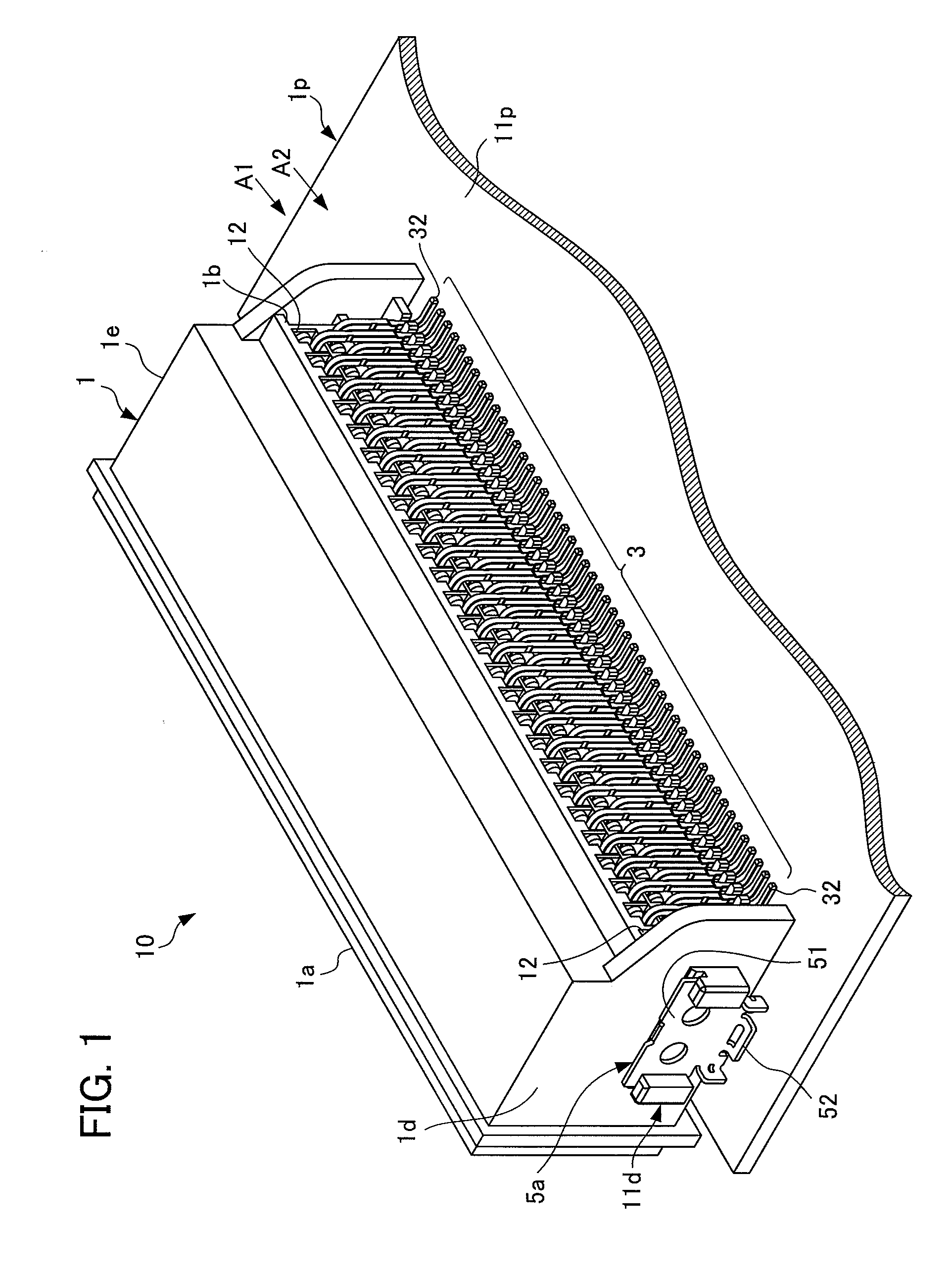
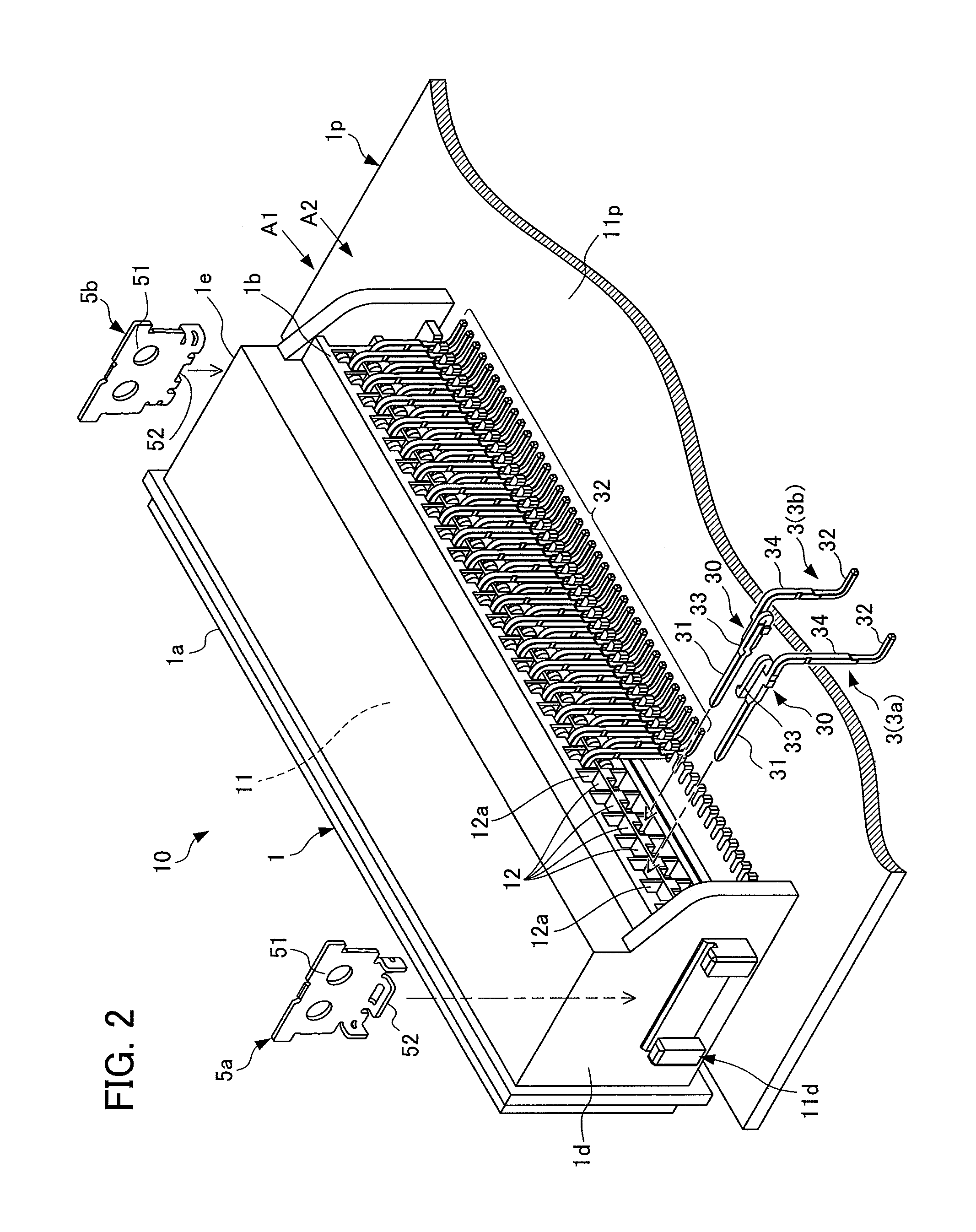
[0046]First, the printed circuit board connector configuration according the first embodiment of the present invention will be explained. FIG. 1 is a perspective view of a printed circuit board connector configuration according to the first embodiment of the present invention with the printed circuit board connector seen from a top surface side. FIG. 2 is an exploded perspective view of the printed circuit board connector configuration according to the first embodiment with the printed circuit board connector seen from a top surface side.

[0047]FIG. 3 is a perspective view of the printed circuit board connector configuration according to the first embodiment with the printed circuit board connector seen from a bottom surface side. FIG. 4 is a perspective view of the printed circuit board connector according to the first embodiment, showing a cross-section of the housing.

[0048]FIG. 5 is a plan view of the printed circuit board connector acc...

second embodiment

Printed Circuit Board Connector Configuration

[0067]The printed circuit board connector configuration according the second embodiment of the present invention will now be explained. FIG. 8 is a perspective view of a printed circuit board connector configuration according to the second embodiment of the present invention with the printed circuit board connector seen from a top surface side. FIG. 9 is an exploded perspective view of the printed circuit board connector configuration according to the second embodiment with the printed circuit board connector seen from a top surface side.

[0068]FIG. 10 is a perspective view of the printed circuit board connector configuration according to the second embodiment with the printed circuit board connector seen from a bottom surface side. FIG. 11 is a longitudinal section profile view of the printed circuit board connector according to the second embodiment cut along a first contact. FIG. 12 is an expanded longitudinal section profile view of an...


PUM


Abstract

A printed circuit board connector is equipped with a housing and plurality of contacts. The housing has an insertion chamber 11 inserted by the mating-side connector, and a plurality of contact-insertion holes inserted by the contacts. The contact has a base portion, a contact-connecting portion that connects with a mating-side contact, and a lead portion that is solder-bonded to the printed circuit board. The base portion and the housing have a contact lance and level that engage with each other so that the contact does not move in an insertion direction to the contact insertion hole or a reverse direction, and the contact lance and level swingably hold the base portion inside the contact-insertion hole so that the lead portion approaches and separates from the printed circuit board surface.

Description

[0001]This application is based on and claims the benefit of priority from Japanese Patent Application No. 2010-276567, filed on 13 Dec. 2010, the content of which is incorporated herein by reference.BACKGROUND OF THE INVENTION[0002]1. Field of the Invention[0003]The present invention relates to printed circuit board connectors. The present invention particularly relates to a printed circuit board connector structure to which a plurality of contact leads can be securely solder-bonded to a printed circuit board surface.[0004]2. Related Art[0005]A shell formed by a metallic plate composes an outer shell of a connector on a printed circuit board connector, for example. A part of the shell is solder-bonded to a surface of the printed circuit board as a reinforcing tab extending from the outer shell to improve connector strength.[0006]However, in a plan view, this kind of reinforcing tab extends outward from the connector shell occupying a certain amount installation space on the printed...

Claims


Application Information

Patent Timeline
Patent Type & Authority Patents(United States)
IPC IPC(8): H01R13/62
CPCH01R13/4223H01R12/724H01R12/7064
Inventor MATSUMOTO, HIROYUKIMASADA, SHINYA
Owner JST MFG CO LTD
Why Eureka
Try Eureka