Apparatus for interfacing circuit domains

a technology of interfacing circuits and circuits, applied in the field of integrated circuits, can solve problems such as local heating or unnecessarily draining batteries, complexity of cross-domain signaling interface circuits, and complex circuits

Active Publication Date: 2013-06-04
ANALOG DEVICES INC
View PDF9 Cites 3 Cited by
  • Summary
  • Abstract
  • Description
  • Claims
  • Application Information

AI Technical Summary

Problems solved by technology

Complexity of cross-domain signaling interface circuits increases as a large number of low voltage precision signal processing circuits are integrated in the same system (or, system on a chip (SoC)) along with the large digital control circuitry, microelectromechanical (MEMS) sensors, and high voltage power drivers.
While this array of different voltage domains enables ambitious applications to be monolithically integrated into the same substrate, it poses challenges to the robustness of the circuit during cross domain powering and cross-domains stress events.
It is possible that the receiving circuit could dissipate large amounts of power if the driving signal is not well-defined, causing localized heating or unnecessarily draining a battery.
If dedicated cross-domain electrostatic (ESD) protection devices are situated between domains to enhance the IC robustness, those devices can actually be overstressed and get damaged, since they are not designed to operate in DC conditions.
However, when a large number of circuit sections co-exist on a mixed-signal IC, the number of level translators needed is proportionally large and can consume a substantial amount of die area with increased cost.
Further, level-translators interpose an additional delay in signal transmission that may be unacceptable for signals with critical timing requirements.
Finally, level translators remain active at all times, thereby increasing power dissipation when the cross-domain signals are actively switching.

Method used


Image

  • Apparatus for interfacing circuit domains
  • Apparatus for interfacing circuit domains
  • Apparatus for interfacing circuit domains

Examples


Embodiment Construction

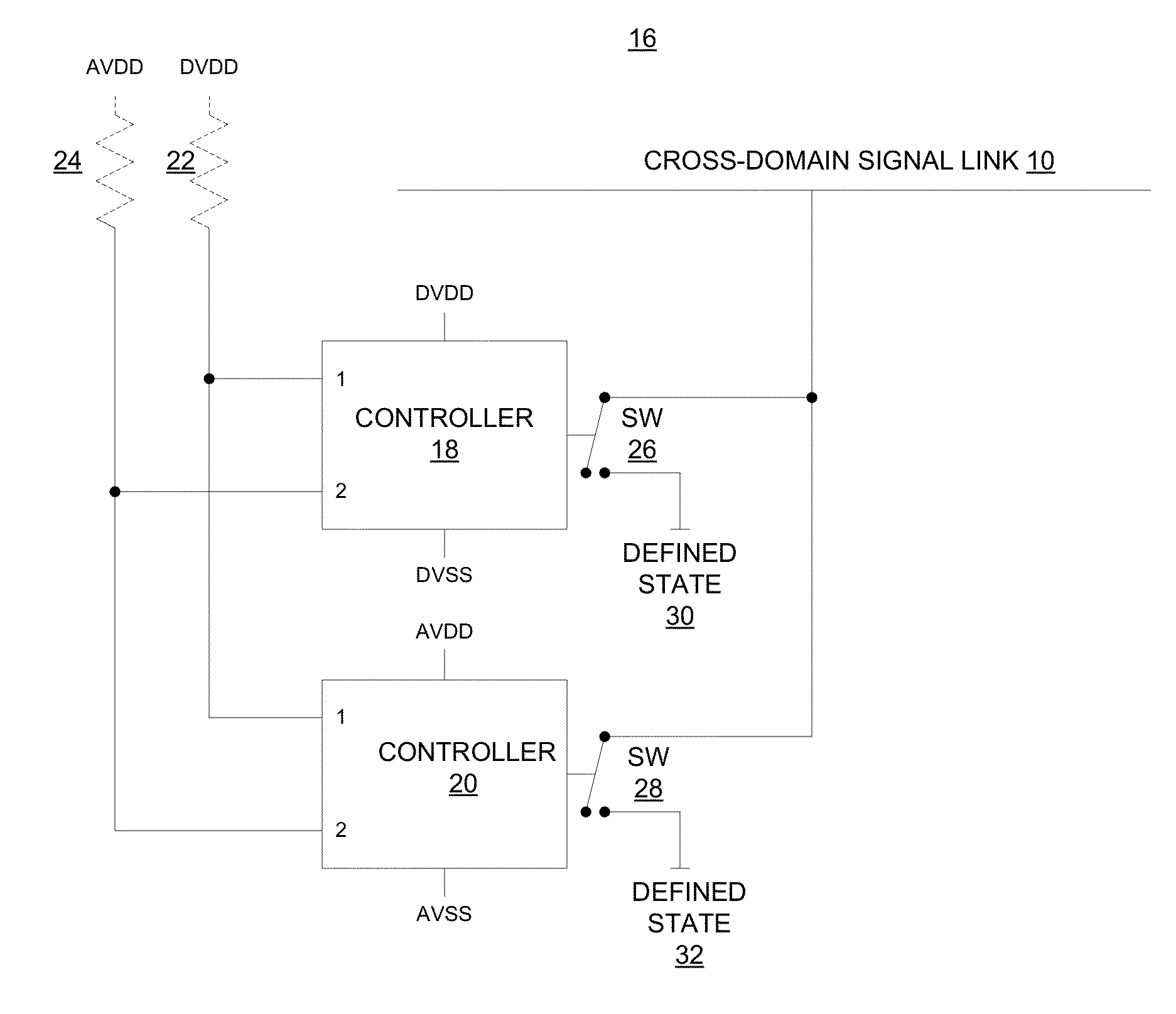
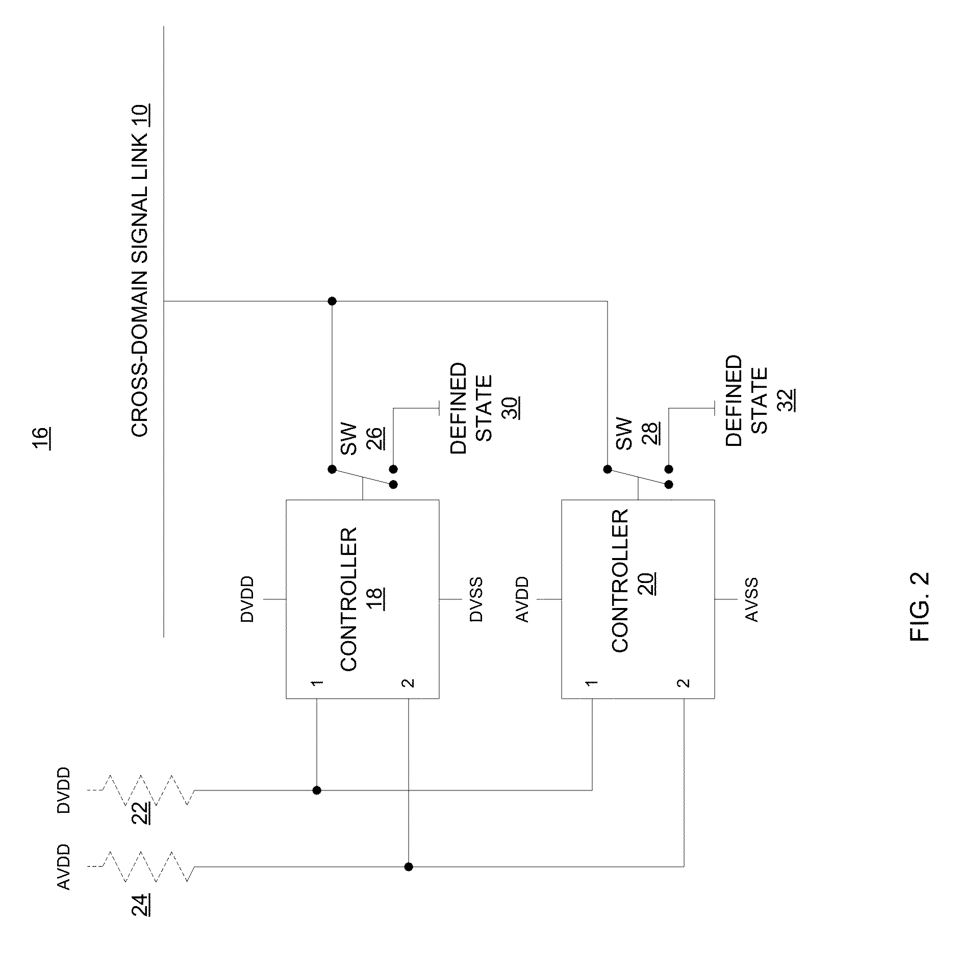
[0019]Thus, there is a need for circuits that control states of cross-domain signal links between circuit domains and that occupy little circuit area, consume minimum power and insert no or little delay to cross-domain signal links and enhance protection robustness in complex SoC. It is one of the objectives of the present invention to ensure that cross-domain signals are held in well-defined logic states until all domains are powered up without using level translators.

[0020]Embodiments of the present invention may include an interface circuit for controlling a cross-domain signal link between a first circuit domain and a second circuit domain in a circuit. The interface circuit may include first and second controllers, each of the first and second controllers including a first input coupled to a first voltage source of the first circuit domain and a second input coupled to a second voltage source of the second circuit domain. The interface circuit may further include a first switch...


PUM


Abstract

An interface circuit for controlling a cross-domain signal link between a first circuit domain and a second circuit domain in a circuit may include first and second controllers, each of the first and second controllers including a first input coupled to a first voltage source of the first circuit domain and a second input coupled to a second voltage source of the second circuit domain. The interface circuit may further include a first switch controlled by an output of the first controller, the first switch including a first end coupled to the cross-domain signal link and a second end coupled to a first defined voltage state, and a second switch controlled by an output of the second controller, the second switch including a first end coupled to the cross-domain signal link and a second end coupled to a second defined voltage state, in which during a power-up of the circuit, if one of the first and second voltage sources is unavailable, at least one of the first and second controllers generates a control signal to engage at least one of the first and second switches and pull the cross-domain signal link to one of the first and second defined voltage states, while providing cross-domain protection against field-induced charge device model (FICDM) stress conditions at small drivers and receiver inputs connected to the signal interface link.

Description

FIELD OF THE INVENTION[0001]The present invention is directed to integrated circuits. In particular, the present invention is directed to interfacing between different power domains in the integrated circuits.BACKGROUND INFORMATION[0002]Large digital and / or mixed-signal integrated circuits (IC) often contain multiple power supply domains. A power supply domain is a block of circuitry that receives the operating power from a unique source of power supply. For example, a mixed-signal chip may use one power supply for the (usually larger) digital section, and a second for the (usually smaller) analog section. This arrangement keeps digital switching noise arising in the digital section from interfering with potentially noise-sensitive analog signals in the analog section. Complexity of cross-domain signaling interface circuits increases as a large number of low voltage precision signal processing circuits are integrated in the same system (or, system on a chip (SoC)) along with the lar...

Claims


Application Information

Patent Timeline
Patent Type & Authority Patents(United States)
IPC IPC(8): H03L5/00
CPCH03K19/017509
Inventor GOLDSTEIN, STEPHANSALCEDO, JAVIER
Owner ANALOG DEVICES INC
Why Eureka
Try Eureka