
Liquid crystal display panel comprising first connecting electrodes disposed on a padding device and electrically connected to active devices and to second connecting electrodes

a technology of liquid crystal display panel and padding device, which is applied in the field of display panel, can solve the problems of affecting the display quality of lcd panel, light leakage in the bright/dark state, etc., and achieve the effect of high contrast and superior display quality

Inactive Publication Date: 2013-04-16
WINTEK CORP
View PDF5 Cites 21 Cited by
  • Summary
  • Abstract
  • Description
  • Claims
  • Application Information

AI Technical Summary

Benefits of technology

This patent is for a liquid crystal display (LCD) panel that has high quality and contrast. The invention solves a problem called dark state light leakage, which occurs when signals from data lines interfere with voltage in the display electrodes. The invention uses shielding electrodes above the data lines to prevent interference and improve the quality of the display. Additionally, the placement of the display electrodes allows for a larger display aperture ratio, resulting in a more visually appealing display.

Problems solved by technology

However, when a distance between the pixel electrodes and the data lines becomes too short, a fringe field between the data lines and the pixel electrodes then influences the tilting of liquid crystal molecules to result in bright / dark state light leakage, thereby affecting the display quality of LCD panels.

Method used


Image

  • Liquid crystal display panel comprising first connecting electrodes disposed on a padding device and electrically connected to active devices and to second connecting electrodes
  • Liquid crystal display panel comprising first connecting electrodes disposed on a padding device and electrically connected to active devices and to second connecting electrodes
  • Liquid crystal display panel comprising first connecting electrodes disposed on a padding device and electrically connected to active devices and to second connecting electrodes

Examples


Embodiment Construction

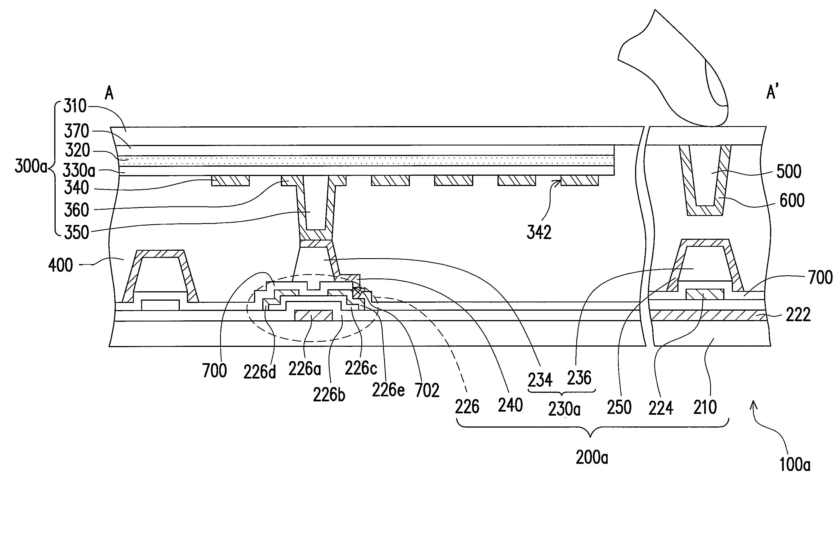
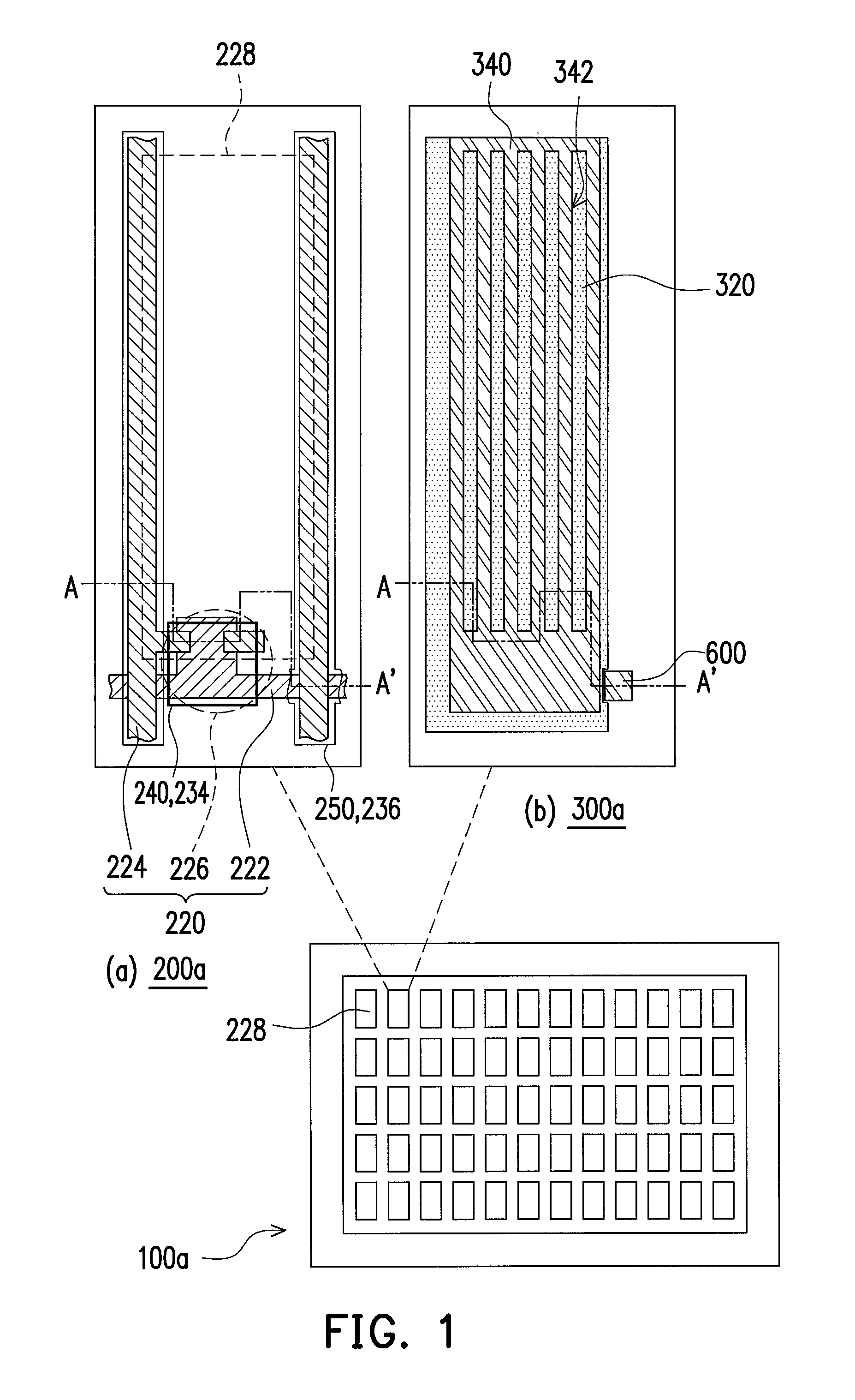
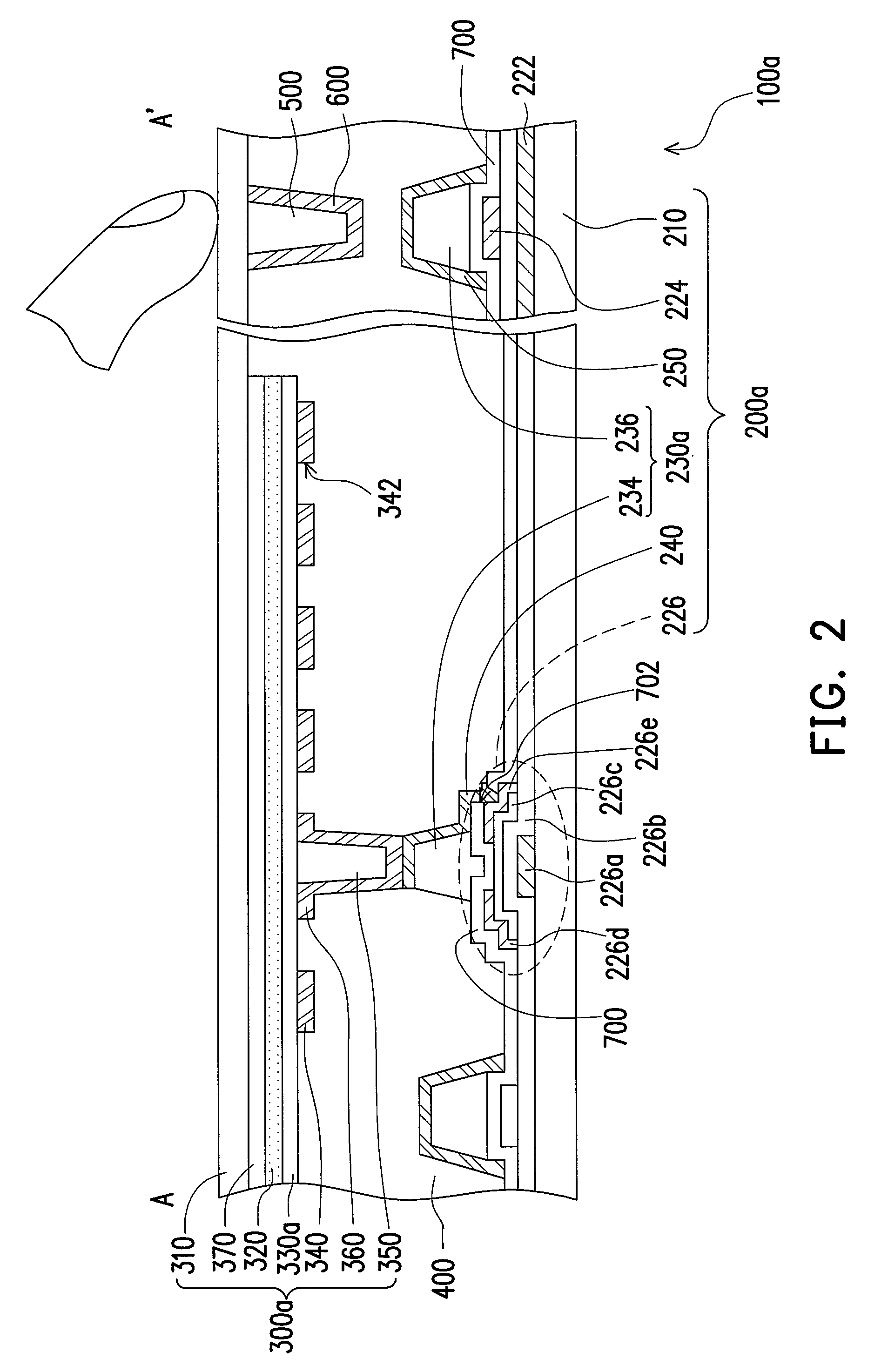
[0016]FIG. 1 is a schematic top view of a liquid crystal display (LCD) panel according to an embodiment of the invention. A sub-diagram (a) illustrates a partial schematic top view of an active device matrix substrate. A sub-diagram (b) illustrates a partial schematic top view of an opposite substrate. FIG. 2 is a partial schematic cross-sectional view of the LCD panel taken along line A-A′ in FIG. 1. Referring to FIGS. 1 and 2 simultaneously, in the present embodiment, an LCD panel 100a includes an active device matrix substrate 200a, an opposite substrate 300a, and a liquid crystal layer 400. The opposite substrate 300a is located above the active device matrix substrate 200a. The liquid crystal layer 400 is disposed between the active device matrix substrate 200a and the opposite substrate 300a.

[0017]The active device matrix substrate 200a includes a first substrate 210, an active device array 220, a padding device 230a, a plurality of first connecting electrodes 240, and a plur...


PUM

PropertyMeasurementUnit
voltageaaaaaaaaaa
widthaaaaaaaaaa
distanceaaaaaaaaaa

Abstract

A liquid crystal display panel including an active device matrix substrate, an opposite substrate, and a liquid crystal layer is provided. The active device matrix substrate includes a first substrate, an active device array, a padding device, first connecting electrodes, and shielding electrodes. The padding device is disposed on active devices and data lines of the active device array. The first connecting electrodes are located above the active devices and electrically connected to the active devices. The shielding electrodes are located above the data lines and electrically connected to a common voltage. The opposite substrate includes a second substrate, first electrodes, an insulating layer, second electrodes having slits and opposite to the first electrodes, spacers corresponding to the active devices, and second connecting electrodes covering the spacers to directly contact with the first connecting electrodes and electrically connected to the first electrodes or the second electrodes.

Description

CROSS-REFERENCE TO RELATED APPLICATION[0001]This application claims the priority benefit of Taiwan application serial no. 98137306, filed on Nov. 3, 2009. The entirety of the above-mentioned patent application is hereby incorporated by reference herein and made a part of this specification.BACKGROUND OF THE INVENTION[0002]1. Field of the Invention[0003]The invention relates to a display panel and more particularly to a liquid crystal display panel.[0004]2. Description of Related Art[0005]In general, liquid crystal displays (LCDs) are mainly constituted by two substrates and a liquid crystal layer disposed therebetween, where a plurality of pixel structures is disposed on one of the substrates to control the arrangement of liquid crystal molecules for display. The pixel structures include a plurality of scanning lines, a plurality of data lines, a plurality of active devices, and a plurality of pixel electrodes. The pixel electrodes are located in the pixel regions intersected by the...

Claims


Application Information

Patent Timeline
Patent Type & Authority Patents(United States)
IPC IPC(8): G02F1/1343G02F1/1333G02F1/1335G02F1/1339
CPCG02F1/13338G02F1/13394G06F3/0412G02F2001/133562G02F2001/13396G02F2001/13398G02F2001/134372G02F2001/136218G02F2202/16G06F3/047G02F1/133562G02F1/13396G02F1/13398G02F1/134372G02F1/136218
Inventor WANG, WEN-CHUNYU, MING-CHANGCHANG, YUNG-CHENGCHANG, TING-YUTSAI, WAN-JEN
Owner WINTEK CORP
Learn More