Driving apparatus
a technology of driving apparatus and motor shaft, which is applied in the field of driving apparatus, can solve the problems of harmful influence on picture quality, low power supply level of potential vs. fluctuation, etc., and achieve the effect of preventing fluctuation of power supply level and preventing degradation of picture quality
- Summary
- Abstract
- Description
- Claims
- Application Information
AI Technical Summary
Benefits of technology
Problems solved by technology
Method used
Image
Examples
first embodiment
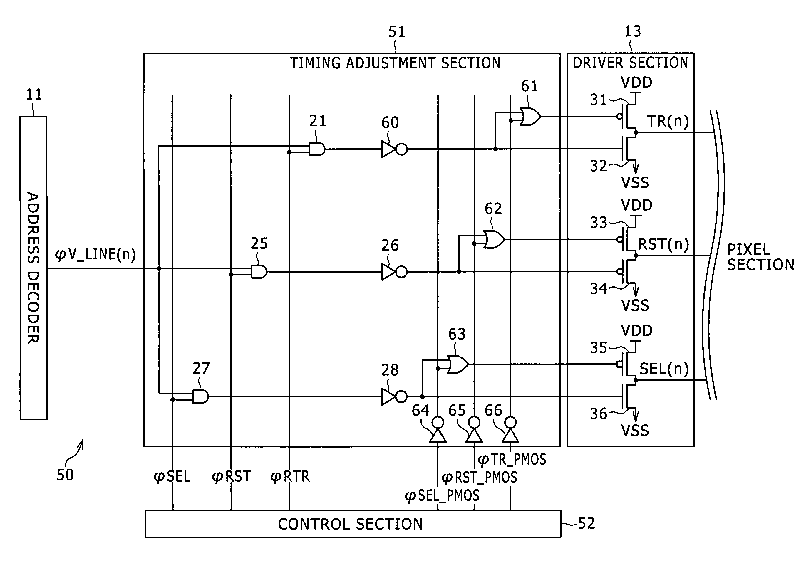
[0053]FIG. 3 shows an example of a configuration of a pixel driving circuit of a CMOS image sensor according to the present invention.
[0054]It is to be noted that, for the convenience of description, a portion of the pixel driving circuit including driving pixels in the nth row is shown in FIG. 3. Further, while, in FIG. 3, an AND circuit, an OR circuit and a NOT circuit are used for simplified illustration, an actual circuit can be implemented using a NAND circuit, a NOR circuit and a NOT circuit. This similarly applies also to a circuit hereinafter described with reference to FIG. 8.
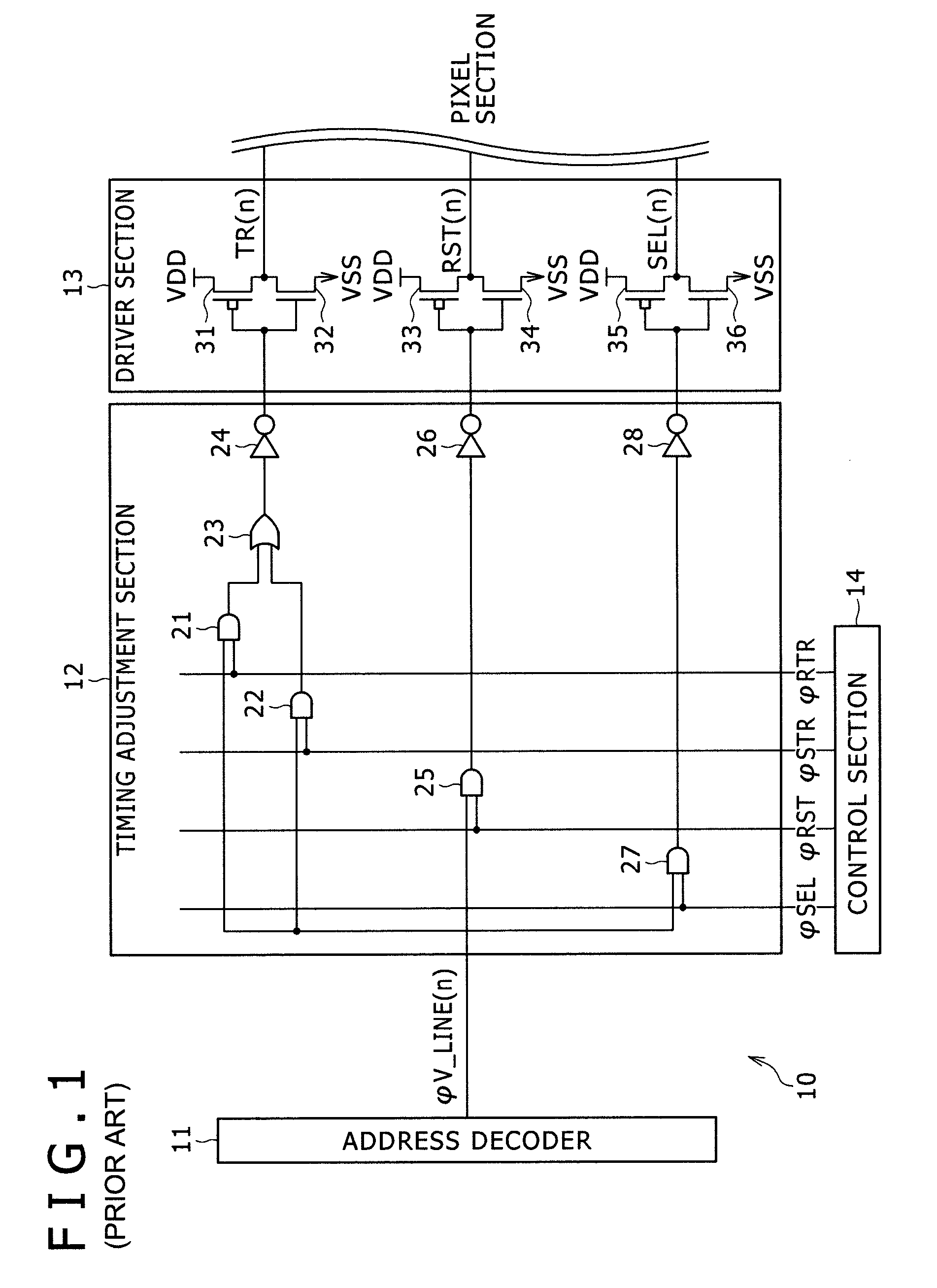
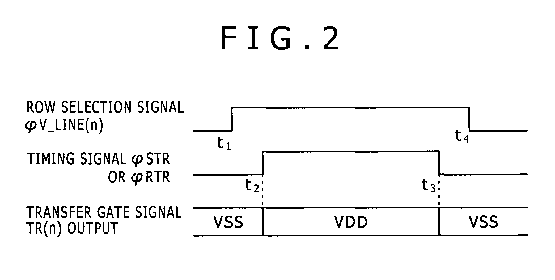
[0055]Referring to FIG. 3, the pixel driving circuit 50 shown includes an address decoder 11, a driver section 13, a timing adjustment section 51 and a control section 52 and produces and outputs a transfer gate signal TR(n), a reset signal RST(n) and a select signal SEL(n). It is to be noted that the pixel driving circuit 50 includes several common components to those described hereinabove with refere...
second embodiment
[0083]FIG. 8 shows an example of a configuration of a pixel driving circuit of a CMOS image sensor according to the present invention.
[0084]Referring to FIG. 8, the pixel driving circuit 100 shown includes an address decoder 11, a timing adjustment section 101, a driver section 102 and a control section 103. The pixel driving circuit 100 produces and outputs a transfer gate signal TR(n), a reset signal RST(n) and a select signal SEL(n) individually having a middle level as well as a transfer gate signal TR(n), a reset signal RST(n) and a select signal SEL(n) individually having the high level or the low level.
[0085]It is to be noted that, while a portion of the pixel driving circuit 100 which produces the transfer gate signal TR(n) is shown in FIG. 8 for the convenience of illustration, also the reset signal RST(n) and the select signal SEL(n) are produced and outputted similarly to the transfer gate signal TR(n). It is to be noted that the pixel driving circuit 100 includes several...
third embodiment
[0110]FIG. 10 shows an example of a configuration of a pixel driving circuit of a CMOS image sensor according to the present invention.
[0111]It is to be noted that a portion of the pixel driving circuit for driving pixels in the nth low is shown in FIG. 10, for the convenience of illustration. Further, while, in FIG. 10, an AND circuit, an OR circuit and a NOT circuit are used for simplified illustration, an actual circuit can be implemented using a NAND circuit, a NOR circuit and a NOT circuit. This similarly applies also to a circuit hereinafter described with reference to FIG. 15.
[0112]The pixel driving circuit 150 in FIG. 10 includes an address decoder 11, a driver section 13, a timing adjustment section 151 and a control section 152, and produces and outputs a transfer gate signal TR(n), a reset signal RST(n) and a select signal SEL(n). It is to be noted that the pixel driving circuit 150 includes several common components to those described hereinabove with reference to FIGS. ...
PUM
 Abstract
Description
Claims
Application Information
 - R&D
- Intellectual Property
- Life Sciences
- Materials
- Tech Scout
- Unparalleled Data Quality
- Higher Quality Content
- 60% Fewer Hallucinations
Browse by: Latest US Patents, China's latest patents, Technical Efficacy Thesaurus, Application Domain, Technology Topic, Popular Technical Reports.
© 2025 PatSnap. All rights reserved.Legal|Privacy policy|Modern Slavery Act Transparency Statement|Sitemap|About US| Contact US: help@patsnap.com


