In-plane switching mode liquid crystal display device
a liquid crystal display and switching mode technology, applied in the field of liquid crystal display devices, can solve the problems of degrading the aperture ratio of the lcd, distortion of the electric field, crosstalk and light leakage, etc., and achieve the effect of enhancing the picture quality of the liquid crystal panel and preventing the degradation of picture quality
- Summary
- Abstract
- Description
- Claims
- Application Information
AI Technical Summary
Benefits of technology
Problems solved by technology
Method used
Image
Examples
first embodiment
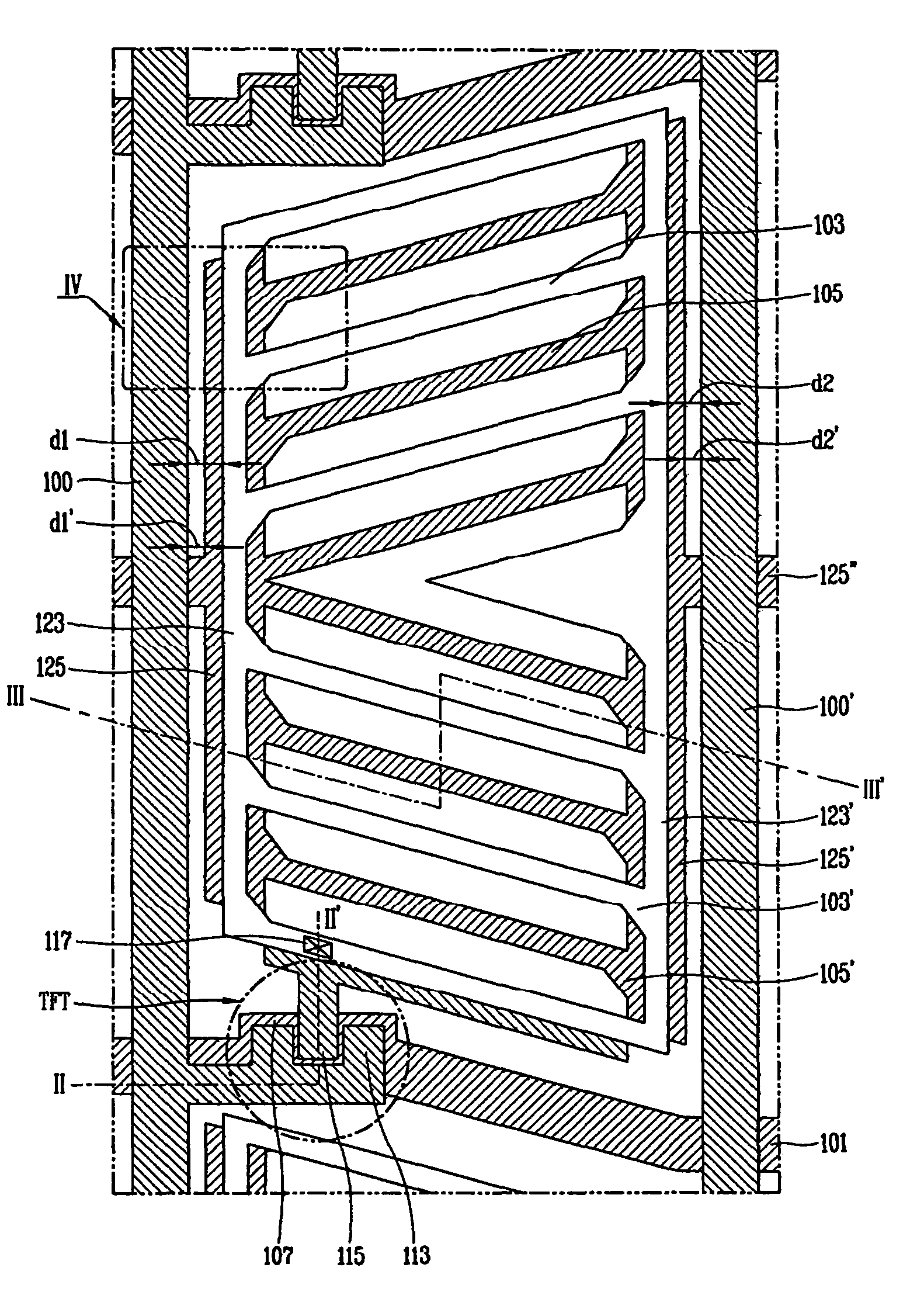
[0041]FIG. 3 shows an exemplary pixel region of an LCD device in accordance with the present invention. FIG. 4A is a cross-sectional view taken along line II-II′ of FIG. 3. FIG. 4B is a cross-sectional view taken along line III-III′ of FIG. 3. Referring to FIGS. 3, 4A and 4B, a liquid crystal panel includes a data line 100 and a gate line 101 arranged on a first substrate 110 and defining a pixel region, a switching device, such as a TFT, disposed at the crossing of the gate line 101 and the data line 100, and at least one pixel electrode 103 and common electrode 105 alternately arranged in parallel in the pixel region to generate in-plane electric field. The pixel electrode 103 and the common electrode 105 are formed to have a tilt angle of about 0°-45° with respect to a direction perpendicular to the data line 100.
[0042]The TFT includes a gate electrode 107 formed as a portion of the gate line 101 on the first substrate 110, a gate insulation film 120 formed on the gate electrode ...
second embodiment
[0052]However, a vertical dim phenomenon may occur in the LCD device due to a parasitic capacitance between the data line 100 and the pixel electrode 103. the present invention is directed to an IPS mode LCD capable of enhancing picture quality of the liquid crystal panel, especially by removing the vertical line phenomenon.
[0053]FIG. 5 shows an exemplary pixel region of an LCD device in accordance with a second embodiment of the present invention. The structure of the second embodiment of the present invention is similar to that of the first embodiment, so only different portions of the second embodiment will be described in further details. The same reference numerals in FIG. 5 refer to the same or like elements of the LCD device of FIG. 3.
[0054]Referring to FIG. 5, a liquid crystal panel includes a data line 100 and a gate line 101 arranged on a first substrate 110 and defining a pixel region, a TFT, namely, a switching device, disposed at the crossing of the gate line 101 and th...
PUM
| Property | Measurement | Unit |
|---|---|---|
| frequency | aaaaa | aaaaa |
| frequency | aaaaa | aaaaa |
| voltages | aaaaa | aaaaa |
Abstract
Description
Claims
Application Information
 - R&D
- Intellectual Property
- Life Sciences
- Materials
- Tech Scout
- Unparalleled Data Quality
- Higher Quality Content
- 60% Fewer Hallucinations
Browse by: Latest US Patents, China's latest patents, Technical Efficacy Thesaurus, Application Domain, Technology Topic, Popular Technical Reports.
© 2025 PatSnap. All rights reserved.Legal|Privacy policy|Modern Slavery Act Transparency Statement|Sitemap|About US| Contact US: help@patsnap.com


