A/D converter unit for image sensor
a converter unit and image sensor technology, applied in the field of a/d converter units for image sensors, can solve the problems of deteriorating performance of a/d conversion, inability to reduce current consumption, so as to achieve the effect of reducing siz
- Summary
- Abstract
- Description
- Claims
- Application Information
AI Technical Summary
Benefits of technology
Problems solved by technology
Method used
Image
Examples
embodiment 1
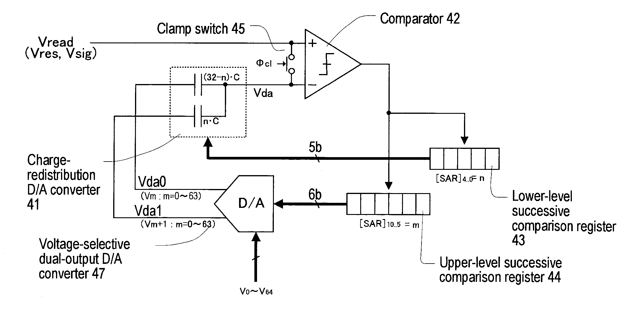
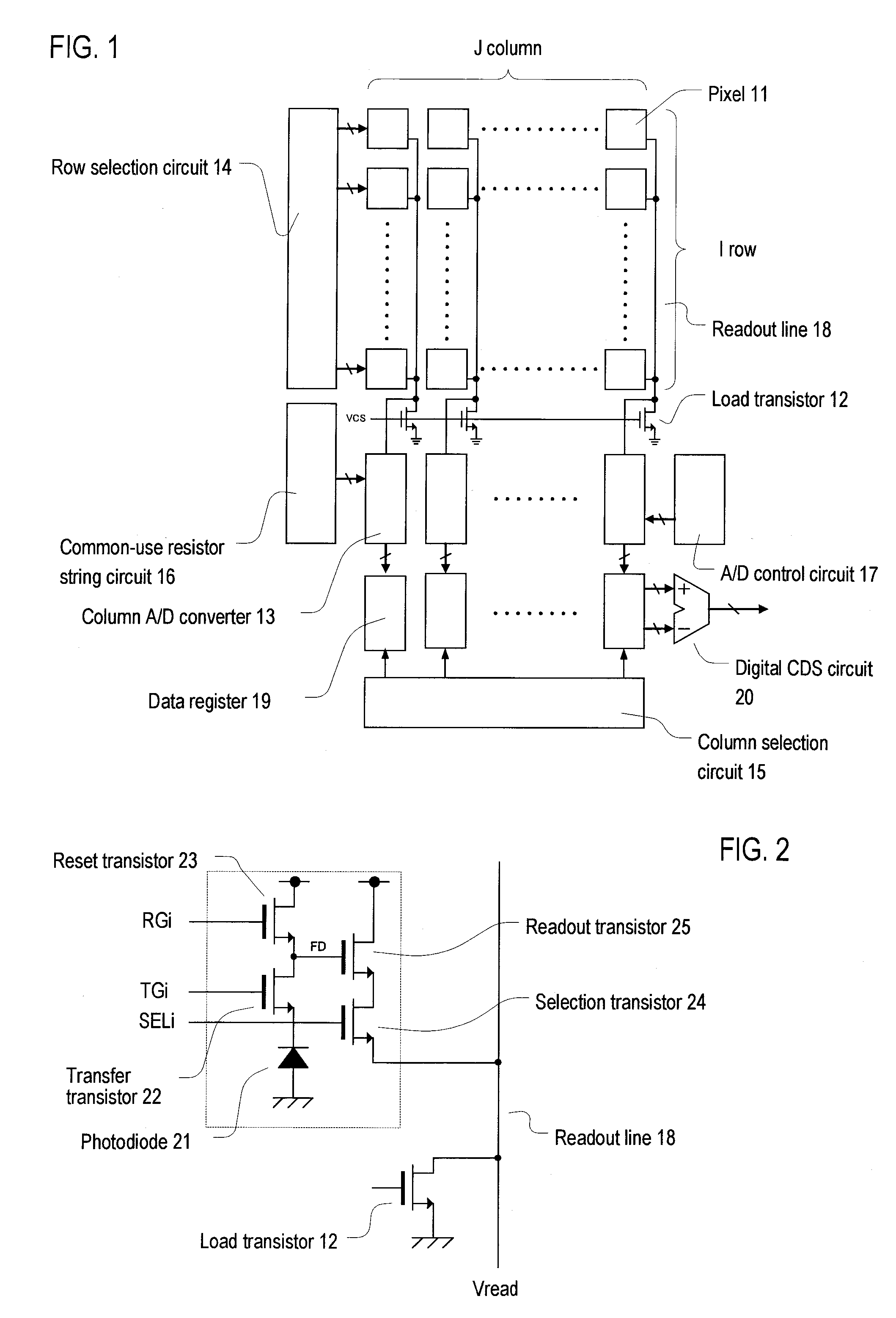
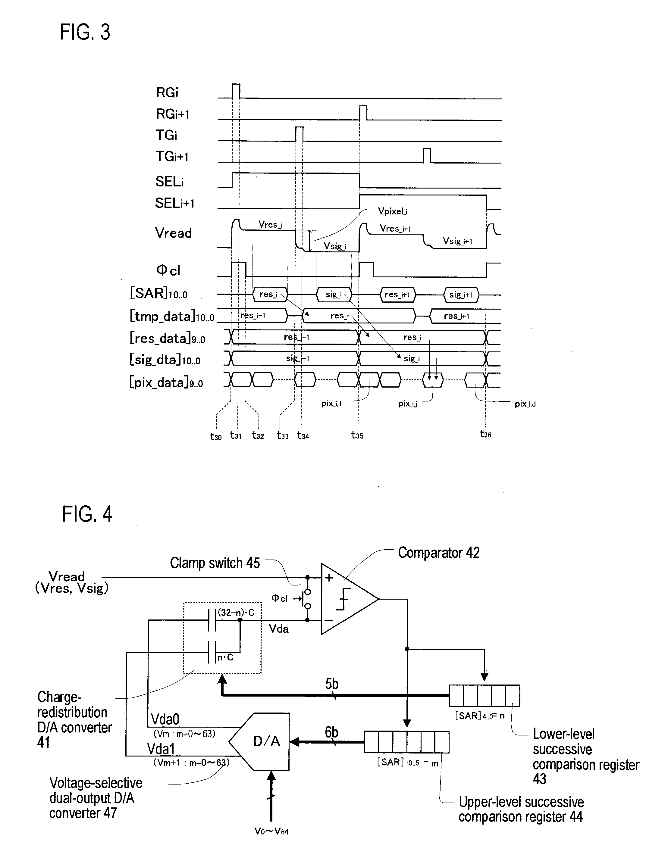
[0038]FIGS. 1 through 12 show an embodiment of the invention, in which like symbols designate like parts. FIG. 1 is a block diagram illustrating an overall configuration of an image sensor according to the present embodiment. A pixel (11) to which photoelectric conversion is to be performed is arranged in a two-dimensional matrix of I rows and J columns. Each pixel in a row selected by a row selection circuit (14) is connected to a readout line (18) of each column. By that a bias current is supplied by a load transistor (12), a signal of the selected pixel is output from a sensor signal output terminal (Vread). In an APS CMOS image sensor, to avoid an influence caused by a pixel-by-pixel difference of readout transistor threshold voltages and a reset noise represented by a kTC noise etc., a signal charge amount stored in a photodiode has to be obtained with accuracy. For this purpose, a method called CDS (Correlated Double Sampling) is generally used, by which a difference is obtain...
PUM
 Abstract
Description
Claims
Application Information
 - R&D
- Intellectual Property
- Life Sciences
- Materials
- Tech Scout
- Unparalleled Data Quality
- Higher Quality Content
- 60% Fewer Hallucinations
Browse by: Latest US Patents, China's latest patents, Technical Efficacy Thesaurus, Application Domain, Technology Topic, Popular Technical Reports.
© 2025 PatSnap. All rights reserved.Legal|Privacy policy|Modern Slavery Act Transparency Statement|Sitemap|About US| Contact US: help@patsnap.com


