Piezoelectric thin film element and piezoelectric thin film device including the same
a piezoelectric thin film and thin film element technology, applied in the direction of device material selection, vacuum evaporation coating, generator/motor, etc., can solve the problems of high dielectric constant of piezoelectric thin film element and the inability to stably produce piezoelectric thin film device using the same, etc., to achieve excellent piezoelectric characteristics, high piezoelectric constant, and long service life
- Summary
- Abstract
- Description
- Claims
- Application Information
AI Technical Summary
Problems solved by technology
Method used
Image


Examples
example 1
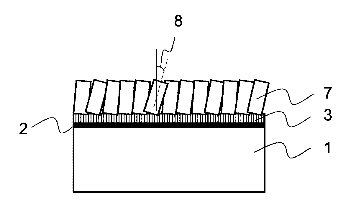
[0095]Example 1 will be described using FIG. 1 to FIG. 5.
[0096]FIG. 1 shows a schematic sectional view of a substrate with a piezoelectric thin film. In this example, the piezoelectric thin film element was manufactured by forming the lower electrode layer 3 and the piezoelectric thin film 4 of potassium sodium niobate having the perovskite structure on the upper part where the bonding layer 2 was formed on the Si substrate 1 having the oxide film. At that time, a crystal orientation state of the piezoelectric thin film was varied depending on manufacturing conditions. A manufacturing method of the piezoelectric thin film element will be described in detail.
[0097]First, the thermal oxide film was formed on the surface of the Si substrate, and the lower electrode layer 3 was formed thereon. The lower electrode layer 3 is composed of a Ti film having thickness of 2 nm formed as a bonding layer 2 and a Pt thin film having thickness of 200 nm formed on the Ti film as the electrode layer...
example 3
[0114]Example 3 will be described using FIG. 8.
[0115]As the example 3, FIG. 8 shows a measurement result of the pole figure of the piezoelectric thin film manufactured by varying the variation of the inclination (off) angles. When the film forming conditions such as the crystal orientation of the Pt lower electrode and the applied electric power for the film deposition of the KNN piezoelectric thin film by sputtering are varied, or when the film forming conditions are not strictly managed, it is clarified that various crystal orientations are shown and the waveform of the Debye rings corresponding to (001) and (111) are variously changed.
[0116]In FIG. 8A, amplitudes of both (001) and (111) are small and the off angles with respect to the substrate are small. Also, it is clarified that the widths of the Debye rings are small, and the KNN thin film is formed, with small off angles and variation with respect to the substrate of the piezoelectric thin film.
[0117]In FIG. 8B, the amplitud...
example 4
[0120]Example 4 will be described using FIG. 9.
[0121]As the example 4, FIG. 9 shows a result of the pole figure measurement of the KNN piezoelectric thin film formed on the Pt lower electrode set in a low orientation state, with sputtering applied electric power varied. In FIG. 9, the inclination (off) angles are varied in accordance with the sputtering applied electric power.
[0122]FIG. 9A shows the pole figure of the KNN thin film when the film deposition is performed, with the sputtering applied electric power set to 60 W, and FIG. 9B shows the pole figure of the KNN thin film when the film deposition is performed, with the sputtering applied electric power set to 65 W. When FIG. 9A and FIG. 9B are compared, the amplitude of the Debye ring of (001) of the KNN thin film formed with applied electric power set to 60 W shown in FIG. 9A is greater than the amplitude when the film deposition is performed with the applied electric power set to 65 W as shown in FIG. 9B. Namely, when the K...
PUM
| Property | Measurement | Unit |
|---|---|---|
| thickness | aaaaa | aaaaa |
| angle | aaaaa | aaaaa |
| smoothness | aaaaa | aaaaa |
Abstract
Description
Claims
Application Information
 - R&D
- Intellectual Property
- Life Sciences
- Materials
- Tech Scout
- Unparalleled Data Quality
- Higher Quality Content
- 60% Fewer Hallucinations
Browse by: Latest US Patents, China's latest patents, Technical Efficacy Thesaurus, Application Domain, Technology Topic, Popular Technical Reports.
© 2025 PatSnap. All rights reserved.Legal|Privacy policy|Modern Slavery Act Transparency Statement|Sitemap|About US| Contact US: help@patsnap.com