Insulated nanogap devices and methods of use thereof
a nano-gap device and isolation technology, applied in the field of nano-gap devices, can solve the problems of limited signal-to-noise issues in the study conducted in aqueous solutions
- Summary
- Abstract
- Description
- Claims
- Application Information
AI Technical Summary
Benefits of technology
Problems solved by technology
Method used
Image


Examples
example 1
Fabrication of Nanogap Devices
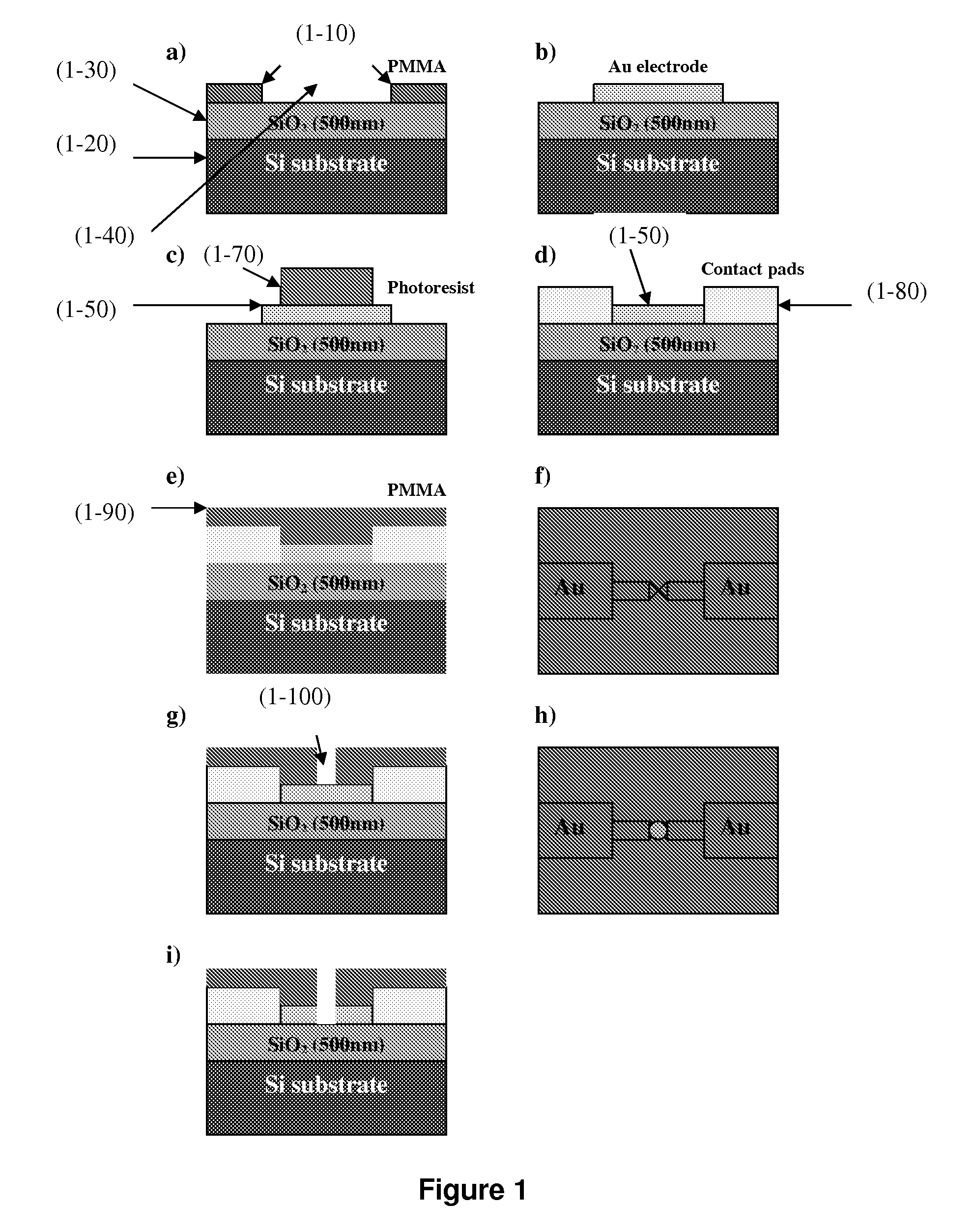
[0219]In one embodiment of the present invention, a nanogap device is fabricated such that all electrical conducting parts in the nanogap device were covered by an insulating polymer layer except in the vicinity of the gap.
[0220]Two techniques were developed to accomplish this design. Thermally assisted electromigration of atoms was used to form a nanogap in a conducting wire and heat generated by joule heating formed a hole in the insulating polymer layer at the position of the nanogap at the same time, using voltage sweep. The technique provides the advantage of great simplicity and versatility, in some embodiments.
[0221]The second technique involved a two step method, where a insulator-coated conducting was utilized and a hole was created in the insulating layer to form the nanogap using selective dissolution of the insulating polymer. This step was followed by feedback-controlled electromigration to form a nanogap. The technique provides an advantag...
example 2
Probing the Electronic Properties of a Single Molecule
[0232]The nanogap devices of the present invention are used to probe the electrical properties of a single molecule or of small aggregates of molecules. A single molecule can be incorporated in the gap during or after the electromigration process. A molecule can be introduced to the gap from a solution of molecules surrounding the gap. An alternate method to incorporate a molecule in the gap is to coat the conducting wire with molecules, prior to coating the wire with the insulating material. When the gap is formed, molecules adjacent to the gap, can fall into the gap or become suspended over the gap. In some embodiments, molecules can bridge the gap, by binding to the two newly-formed electrodes. According to this aspect, and in some embodiments, molecules can comprise one or two functional end groups that adhere to the electrode material. In some embodiments, trapping of molecules in the gap can be accomplished via self-assembl...
example 3
Nanoparticle Size Distribution Determination
[0237]A nanogap device is constructed with a large array of electrode pairs, for example as described in Example 1. Voltage conditions are controlled such that the gap in each electrode pair or in each series of electrode pairs differ from another electrode pair or pairs in the array. The difference in gap size may be controlled and varied with accurate increments of, for example, 0.5 nm. Each electrode pair may be individually addressed by a voltage source and a current analyzer. A series of conducting nanoparticles having a desired size distribution may be introduced to the device from solution. The particles are coated with a functional group that promotes binding to the gap between the electrodes. The number of electrical junctions shortened by the binding of the particles is measured, and the gap size of each shortened junction is recorded. The distribution of shortened junctions and their sizes is used to evaluate the size distributi...
PUM
| Property | Measurement | Unit |
|---|---|---|
| width | aaaaa | aaaaa |
| size | aaaaa | aaaaa |
| nanogap size | aaaaa | aaaaa |
Abstract
Description
Claims
Application Information
 - R&D
- Intellectual Property
- Life Sciences
- Materials
- Tech Scout
- Unparalleled Data Quality
- Higher Quality Content
- 60% Fewer Hallucinations
Browse by: Latest US Patents, China's latest patents, Technical Efficacy Thesaurus, Application Domain, Technology Topic, Popular Technical Reports.
© 2025 PatSnap. All rights reserved.Legal|Privacy policy|Modern Slavery Act Transparency Statement|Sitemap|About US| Contact US: help@patsnap.com