Display device comprising a protective fixing member disposed only about a periphery of a semiconductor chip wherein a top side and a bottom side are co-planar with a respective top side and a bottom side of the semiconductor chip
a protective fixing member and semiconductor chip technology, applied in the field of display devices, can solve the problems of reducing the height presenting an obstacle to efforts to make the portable terminal low in profile, and no consideration for the mounting of the cog chip
- Summary
- Abstract
- Description
- Claims
- Application Information
AI Technical Summary
Benefits of technology
Problems solved by technology
Method used
Image
Examples
first embodiment
[0054](First Embodiment)
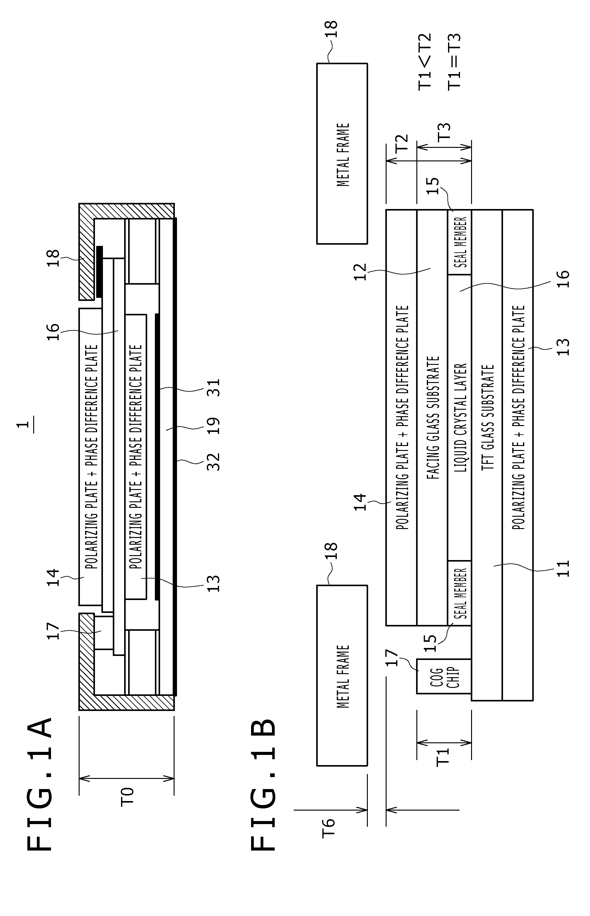
[0055]FIGS. 1A and 1B show in cross section a liquid crystal display device according to a first embodiment of the present invention. Specifically, FIG. 1A shows an overall cross-sectional structure of a liquid crystal panel of the liquid crystal display device according to the first embodiment, and FIG. 1B shows the cross-sectional structure in greater detail. According to the first embodiment, the liquid crystal panel has a liquid crystal layer as a material layer having an electrooptical effect.
[0056]As shown in FIGS. 1A and 1B, the liquid crystal display device, generally denoted by 1, includes a TFT (Thin Film Transistor) glass substrate 11 as a first transparent insulating substrate supporting thereon pixel switches and a driver circuit therefor which are constructed of TFTs, a facing glass substrate 12 as a second transparent insulating substrate disposed in facing relation to the TFT glass substrate 11, polarizing plate and phase difference plate comb...
second embodiment
[0074](Second Embodiment)
[0075]FIG. 5 shows in cross section a liquid crystal display device according to a second embodiment of the present invention.
[0076]As shown in FIG. 5, the liquid crystal display device, generally denoted by 2, includes: a TFT glass substrate 21 as a first transparent insulating substrate supporting thereon pixel switches and a driver circuit therefor which are constructed of TFTs; a facing glass substrate 22 as a second transparent insulating substrate disposed in facing relation to the TFT glass substrate 21; a liquid crystal layer 26 positioned between the TFT glass substrate 21 and the facing glass substrate 22 and having peripheral edges sealed by a seal member 25; polarizing plate and phase difference plate combinations 23, 24 disposed between the TFT glass substrate 21 and the liquid crystal layer 26 and between the liquid crystal layer 26 and the facing glass substrate 22; the liquid crystal layer 26 being held between the polarizing plate and phase ...
PUM
| Property | Measurement | Unit |
|---|---|---|
| total thickness | aaaaa | aaaaa |
| total thickness | aaaaa | aaaaa |
| total thickness T2 | aaaaa | aaaaa |
Abstract
Description
Claims
Application Information
 - R&D
- Intellectual Property
- Life Sciences
- Materials
- Tech Scout
- Unparalleled Data Quality
- Higher Quality Content
- 60% Fewer Hallucinations
Browse by: Latest US Patents, China's latest patents, Technical Efficacy Thesaurus, Application Domain, Technology Topic, Popular Technical Reports.
© 2025 PatSnap. All rights reserved.Legal|Privacy policy|Modern Slavery Act Transparency Statement|Sitemap|About US| Contact US: help@patsnap.com


