Managing the operation of a semiconductor device under varying load conditions

a technology of semiconductor devices and load conditions, applied in the direction of semiconductor/solid-state device details, process and machine control, instruments, etc., can solve the problems of varying the temperature difference between the temperature of the case at the location of the temperature sensor and the actual junction temperature, and the failure of the semiconductor device to overheat and fail, etc., to achieve the effect of reducing the number of transistors

Inactive Publication Date: 2012-09-04
ENGILITY LLC +1
View PDF3 Cites 9 Cited by
  • Summary
  • Abstract
  • Description
  • Claims
  • Application Information

AI Technical Summary

Benefits of technology

[0012]The present invention additionally provides a system for performing the above-described method and computer readable storage media including co

Problems solved by technology

After prolonged continuous usage, the temperature of an operating semiconductor device, such as a power amplifier, may rise to such an extent that the semiconductor device overheats and fails.
While such a measurement provides an approximate measurement of the junction temperature, the difference between the temperature of the case at the location of the temperature sensor and the actual junction temperature varies under varying operating conditions of the semiconductor device because such difference is affected by the power dissipation of the semiconductor device.
However, because TJMAX is specified as an absolute maximum by the semiconductor manufacturer, the sensor temperature cutback threshold (TCB) must be overly conservative to account for the worst case power dissipation conditions which vary as the load changes for static thermal management implementations.
Also, since power dissipation is estimated to be the difference between the power supplied to the semiconductor device and the power delivered by the semiconductor device to the load, it is difficult to quantify power dissipation for non-sinusoidal time-varying signals, modulated signals, and loads that cause reflected power at high frequencies.

Method used


Image

  • Managing the operation of a semiconductor device under varying load conditions
  • Managing the operation of a semiconductor device under varying load conditions
  • Managing the operation of a semiconductor device under varying load conditions

Examples


Embodiment Construction

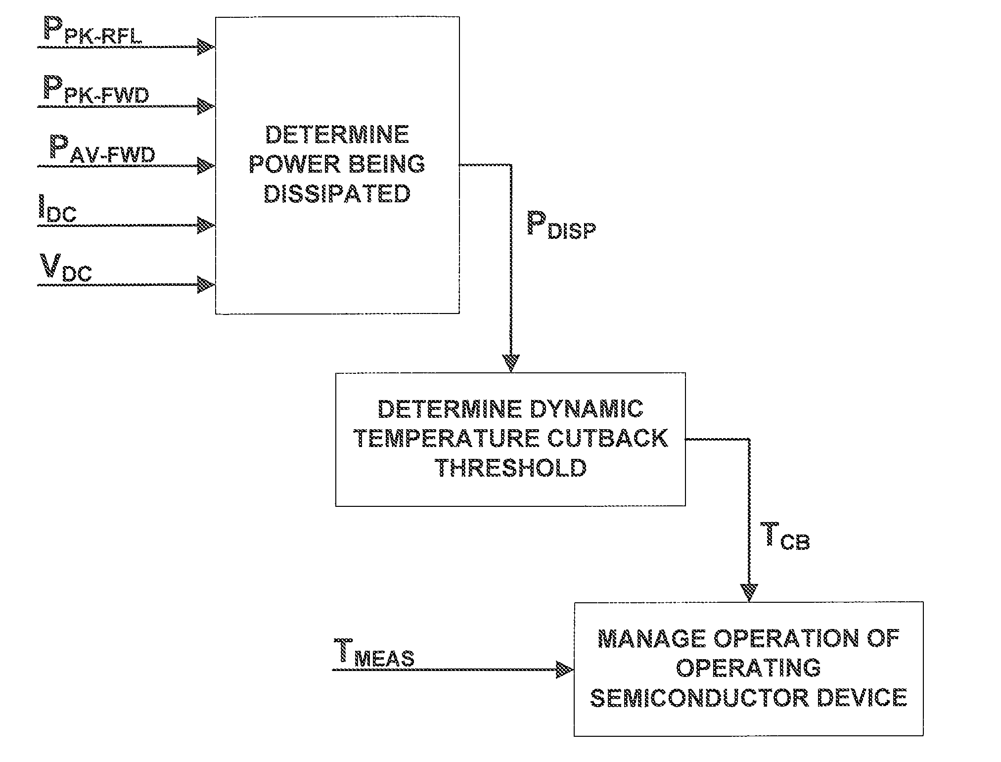
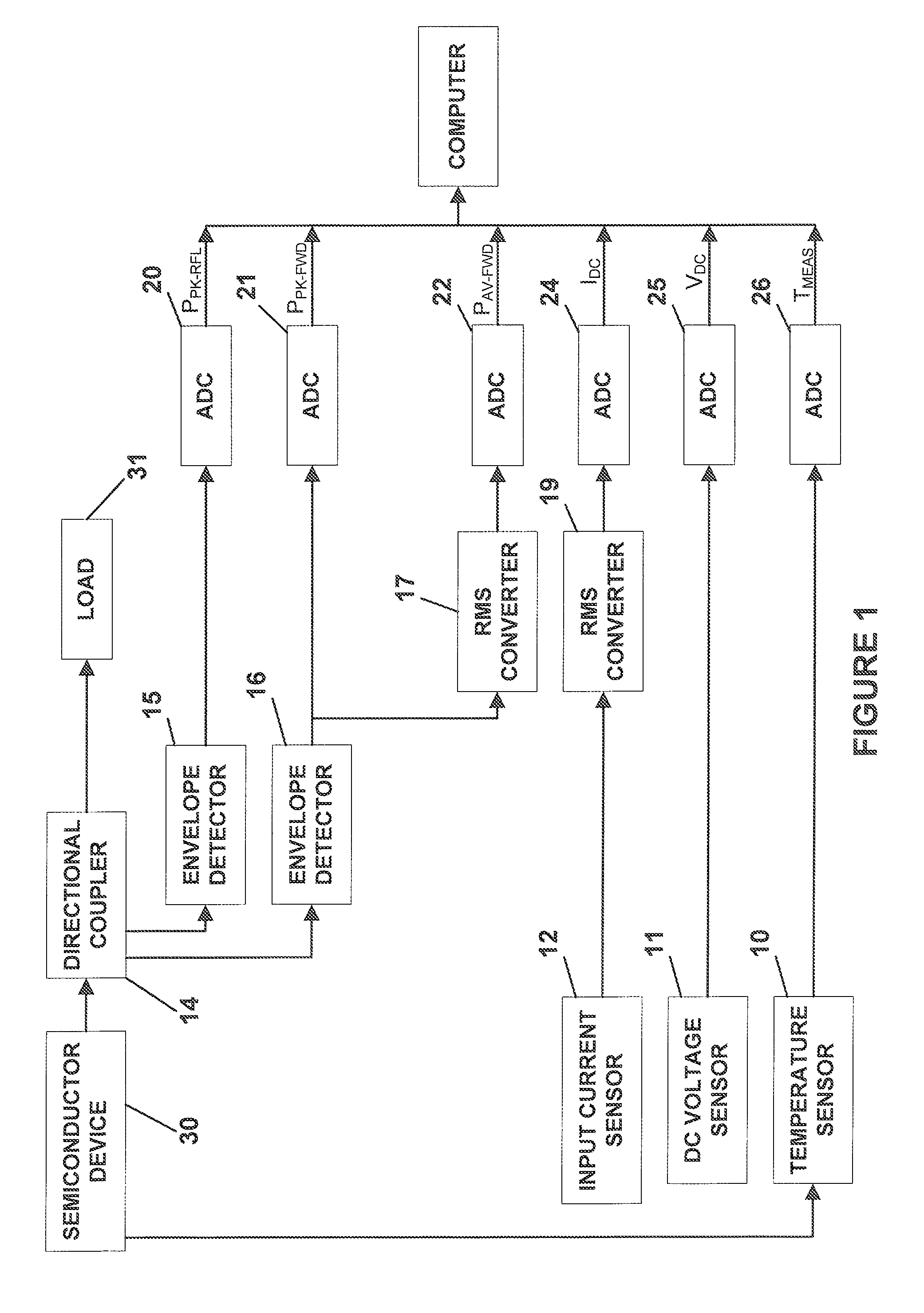
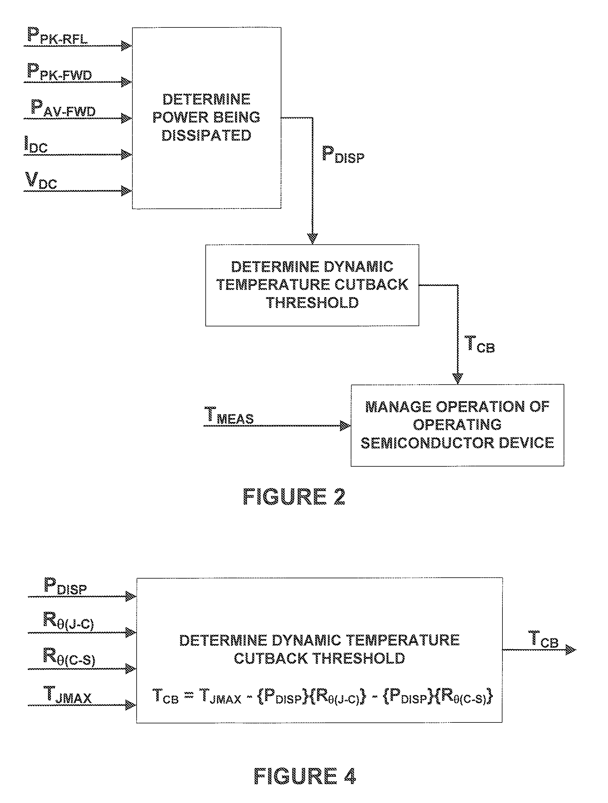
[0019]Referring to FIG. 1, an exemplary embodiment of a system according to the present invention includes a temperature sensor 10, a DC voltage sensor 11, an input current sensor 12, a directional coupler 14, a first envelope detector 15, a second envelope detector 16, a first RMS converter 17, a second RMS converter 19, a set of analog-to-digital converters (ADC) 20, 21, 22, 24, 25, 26 and a computer 27. This exemplary embodiment manages the operation of a semiconductor device 30, such as an RF power amplifier, that is providing power to a load 31, such as an antenna.

[0020]The temperature sensor 10 is coupled to the case of the semiconductor device 30 for measuring a temperature related to the junction temperature of the semiconductor device 30. In some embodiments, the temperature sensor 10 is mounted on the case of semiconductor device. In other embodiments the temperature sensor 10 is mounted adjacent the case of the semiconductor device 30 on a common heatsink.

[0021]The DC vol...


PUM


Abstract

A system for managing the operation of a semiconductor device in accordance with varying load conditions that affect the power being dissipated by the semiconductor device, includes a sensor for measuring a temperature related to the junction temperature of an operating semiconductor device; electronic components for measuring the real-time operating load conditions of the operating semiconductor device; and a computer that is adapted by computer executable program instructions to perform the steps of:(a) determining the power being dissipated by the operating semiconductor device in accordance with the measured real-time operating load conditions of the semiconductor device;(b) determining a dynamic temperature cutback threshold for the operating semiconductor device in accordance with the determination of the power being dissipated; and(c) managing the operation of the semiconductor device in accordance with the measured temperature and the dynamic temperature cutback threshold.

Description

BACKGROUND OF THE INVENTION[0001]The present invention pertains to managing the operation of a semiconductor device under varying load conditions that affect the power being dissipated by the semiconductor device.[0002]The power dissipated by a semiconductor device is dissipated as heat, which causes the temperature of the semiconductor device to rise. After prolonged continuous usage, the temperature of an operating semiconductor device, such as a power amplifier, may rise to such an extent that the semiconductor device overheats and fails. In order to prevent such failure, the operation of the semiconductor device is managed by determining the junction temperature of the semiconductor device and cutting back or interrupting the operation of the semiconductor device when the junction temperature reaches a specified maximum attainable junction temperature (TJMAX) for the semiconductor device. The junction temperature is the temperature at the junction of the output transistor of the...

Claims


Application Information

Patent Timeline
IPC IPC(8): G05D23/00G06F1/00
CPCH01L23/34H01L2924/0002H01L2924/00
Inventor O'BRIEN, THOMAS DANIELRODZINKA, MARK DAVIDTRABOLD, JOSEPH GERARD
Owner ENGILITY LLC
Why Eureka
Try Eureka