
CMOS image sensor

a technology of image sensor and cmos, which is applied in the field of cmos image sensor, can solve the problem of three-times as much power as cmos image sensor, and achieve the effect of improving low exposure and high exposure quality of imag

Inactive Publication Date: 2012-08-21
ELECTRONICS & TELECOMM RES INST
View PDF17 Cites 5 Cited by
  • Summary
  • Abstract
  • Description
  • Claims
  • Application Information

AI Technical Summary

Benefits of technology

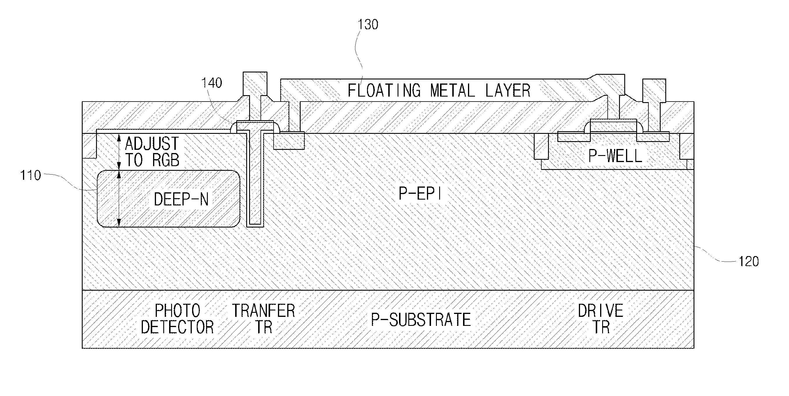
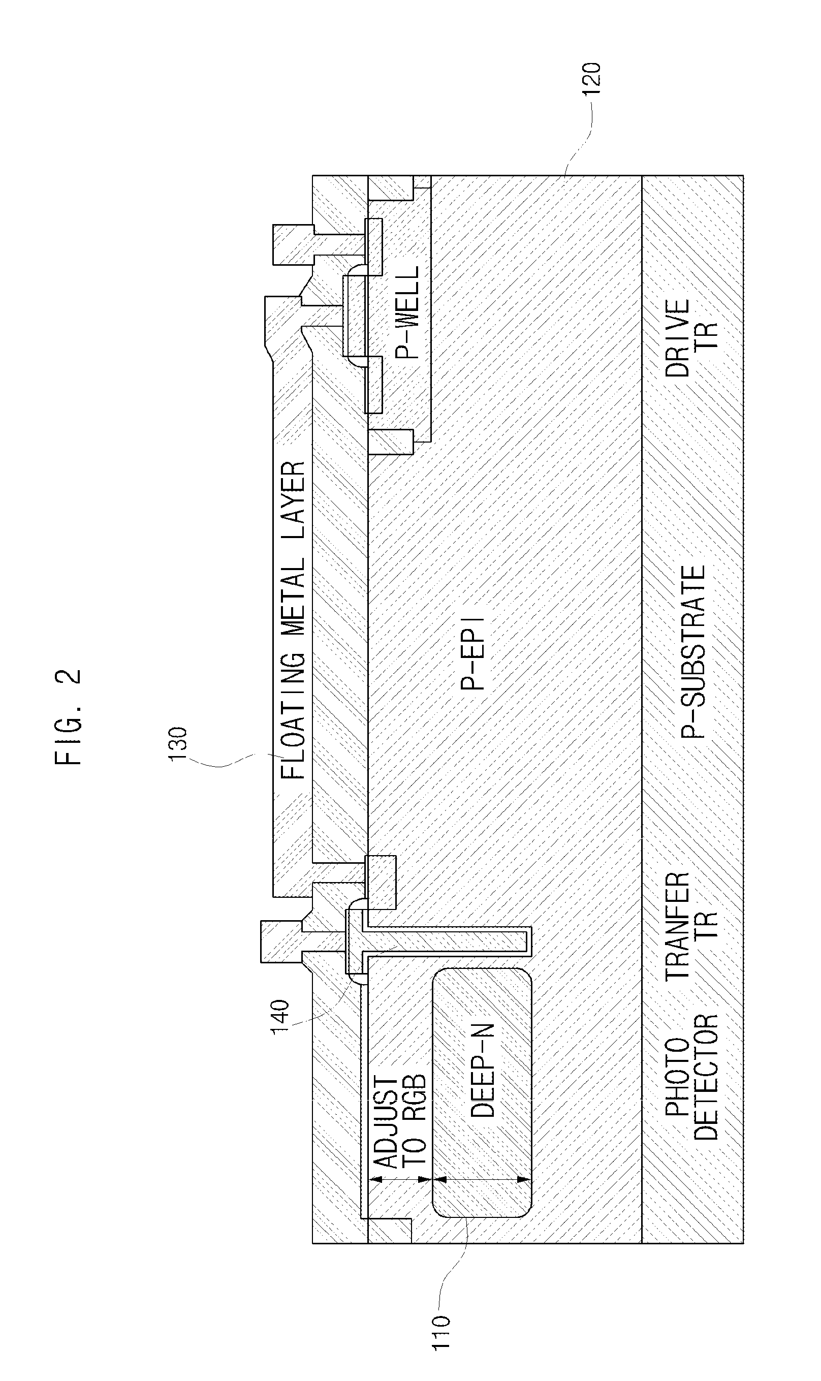
[0008]In order to solve the above problems, it is an object of the present invention to provide a CMOS image sensor capable of improving low exposure and high exposure quality of image by changing a cell structure and a doping concentration and a manufacturing method thereof.

Problems solved by technology

However, the CCD type image sensor requires driving powers of different levels 14 V, 3.3 V, −8 V and consumes power three times as much as the CMOS image sensor.

Method used


Image

  • CMOS image sensor
  • CMOS image sensor
  • CMOS image sensor

Examples


Embodiment Construction

[0016]Advantages and features of the present invention and methods to achieve them will be elucidated from exemplary embodiments described below in detail with reference to the accompanying drawings. However, the present invention is not limited to exemplary embodiment disclosed herein but will be implemented in various forms. The exemplary embodiments are provided by way of example only so that a person of ordinary skill in the art can fully understand the disclosures of the present invention and the scope of the present invention. Therefore, the present invention will be defined only by the scope of the appended claims. Meanwhile, terms used in the present invention are to explain exemplary embodiments rather than limiting the present invention. In the specification, a singular type may also be used as a plural type unless stated specifically. “Comprises” and / or “comprising” used herein does not exclude the existence or addition of one or more other components, steps, operations a...


PUM


Abstract

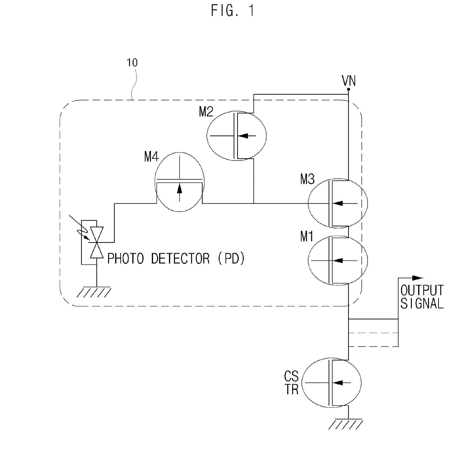
Disclosed is a CMOS image sensor and a manufacturing method thereof. According to an aspect of the present invention, each pixel of CMOS image sensor includes a photo detector that includes an electon Collection layer doped with a concentration of 5×10¹⁵ / cm3 to 2×10¹⁶ / cm3; and a transfer transistor that is connected to the photo detector and is formed of a vertical type trench gate of which the equivalent oxide thickness is 120 Å or more.

Description

CROSS-REFERENCE TO RELATED APPLICATIONS[0001]This application claims priority under 35 U.S.C. §119 to Korean Patent Application No. 10-2010-0034426, filed on Apr. 14, 2010, and Korean Patent Application No. 10-2009-0095776, filed on Oct. 8, 2009, in the Korean Intellectual Property Office, the disclosure of which is incorporated herein by reference in its entirety.BACKGROUND OF THE INVENTION[0002]1. Field of the Invention[0003]The present invention relates to a CMOS image sensor, and more particularly, to a CMOS image sensor capable of improving low exposure and high exposure qualities of image and a manufacturing method thereof.[0004]2. Description of the Related Art[0005]Recently, CCD or CMOS type image sensors have been developed by companies, such as Omnivision, Micron, Foveon, Sony, Samsung Electrionics, Dongbu hightec, Magnachip, etc.[0006]The former CCD type image sensor has been developed by a Long Electron Life Time technology, a Double poly technology, and a High Voltage s...

Claims


Application Information

Patent Timeline
Patent Type & Authority Patents(United States)
IPC IPC(8): H01L31/062
CPCH01L27/1461H01L27/14614H01L27/14645H01L27/14689
Inventor KANG, JIN YEONG
Owner ELECTRONICS & TELECOMM RES INST
Learn More