
Pixel and organic light emitting display using the same

a technology of organic light and display, applied in static indicating devices, electroluminescent light sources, instruments, etc., can solve the problems of oled deformation and inability to display images with desired luminance, and achieve the effect of stably compensating

Active Publication Date: 2012-08-14
SAMSUNG DISPLAY CO LTD
View PDF13 Cites 7 Cited by
  • Summary
  • Abstract
  • Description
  • Claims
  • Application Information

AI Technical Summary

Benefits of technology

[0022]The pixel and the organic light emitting display using exemplary embodiments of the present invention compensate for deterioration of the organic light emitting diode, making it possible to display an image with a desired luminance. Also, according to exemplary embodiments of the present invention, even when the position of the pixels is differently set due to the voltage falling of the second power supply ELVSS, the deterioration of the organic light emitting diode can be stably compensated.

Problems solved by technology

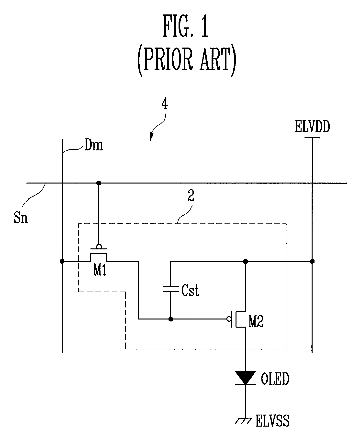
However, there is a problem that the conventional organic light emitting display cannot display an image with desired luminance when there is an efficiency change as a result of deterioration of the OLED.
In other words, the OLED degrades with time and the conventional organic light emitting display cannot display an image with a desired luminance as a result of the degradation.

Method used


Image

  • Pixel and organic light emitting display using the same
  • Pixel and organic light emitting display using the same
  • Pixel and organic light emitting display using the same

Examples


Embodiment Construction

[0028]In the following detailed description, only certain exemplary embodiments of the present invention are shown and described, by way of illustration. As those skilled in the art would recognize, the invention may be embodied in many different forms and should not be construed as being limited to the embodiments set forth herein. Like reference numerals designate like elements throughout the specification.

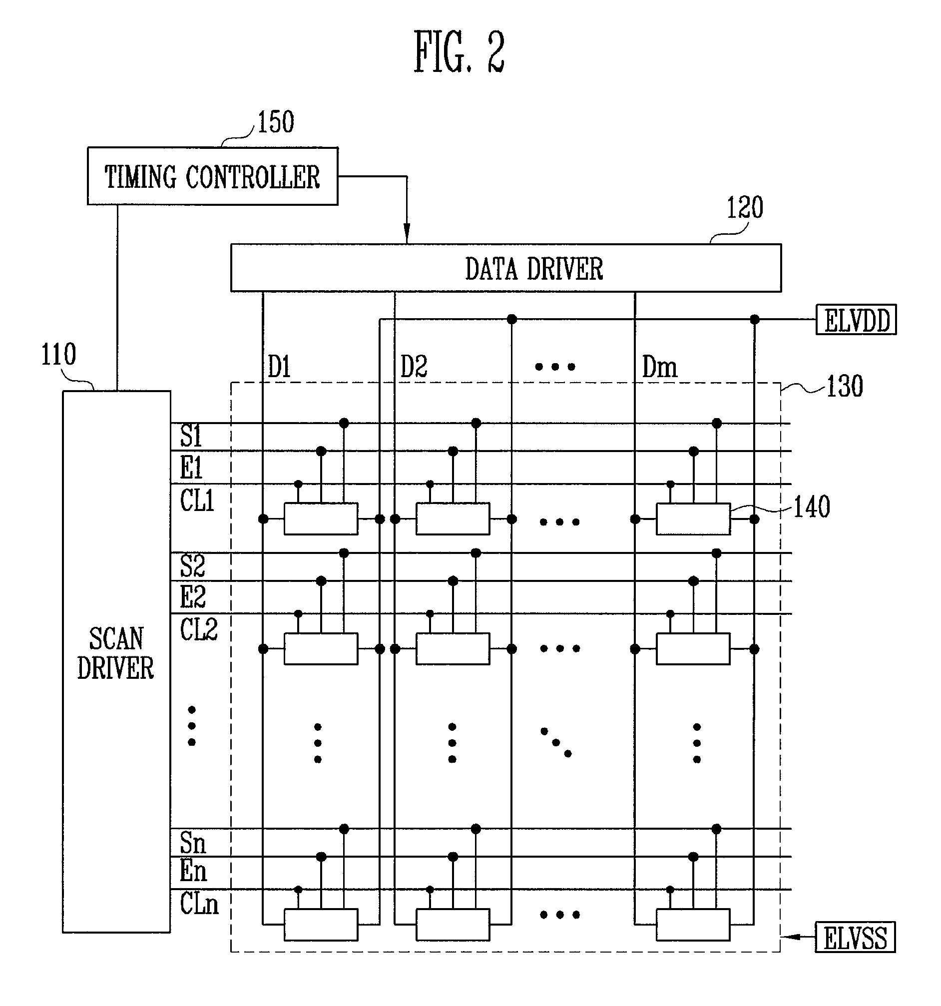
[0029]FIG. 2 illustrates an organic light emitting display according to an exemplary embodiment of the present invention. The organic light emitting display includes a display area / region (or pixel unit) 130, a scan driver 110, a data driver 120, and a timing controller 150. The display area 130 includes pixels 140 at crossing regions (or intersection parts) of scan lines S1 to Sn, light emitting control lines E1 to En, control lines (or first control lines) CL1 to CLn, and data lines D1 to Dm. The scan driver 110 drives the scan lines S1 to Sn, the light emitting control lines ...


PUM


Abstract

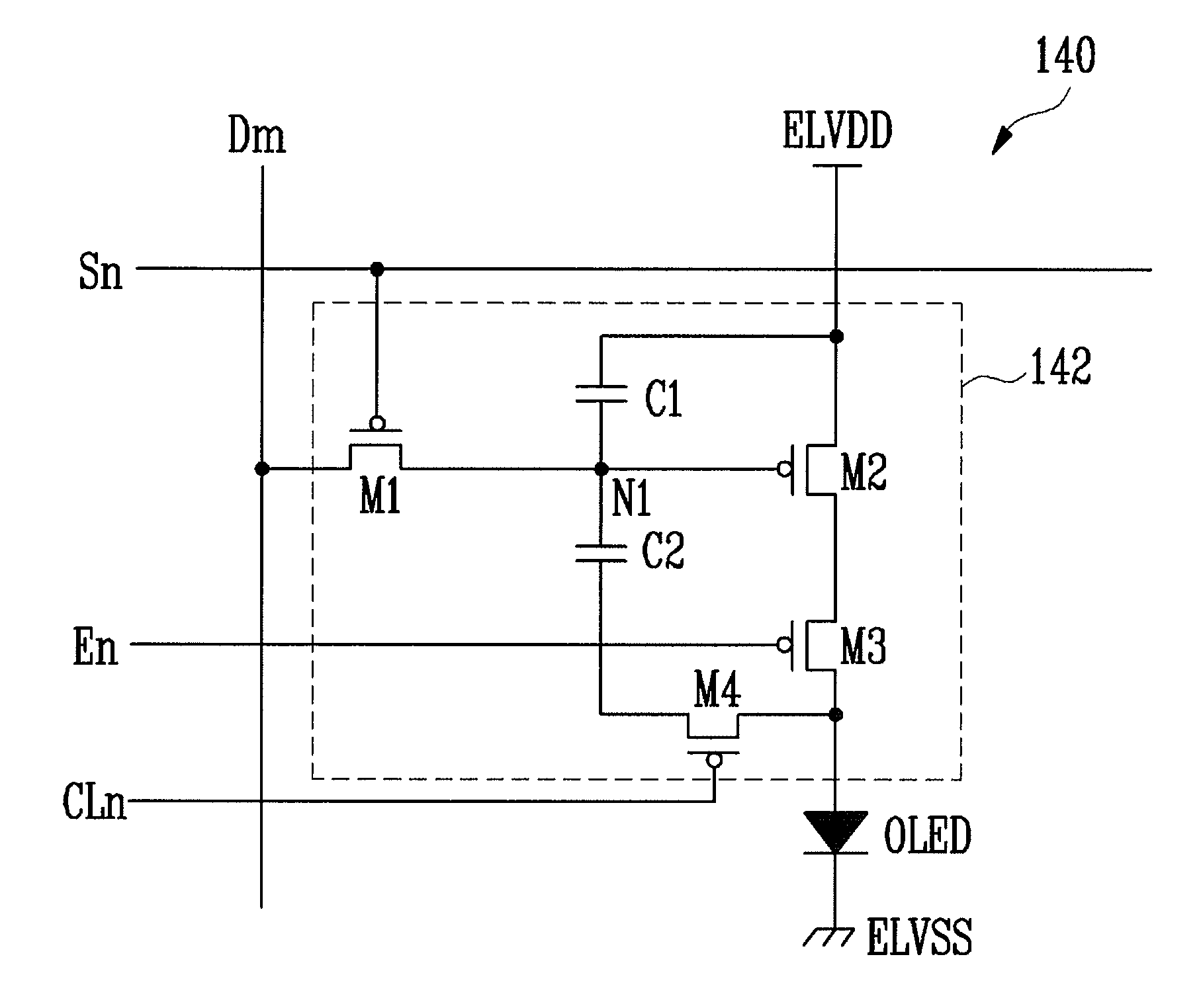
A pixel is provided including an OLED having anode and cathode electrodes. A second transistor controls current supplied from a first power supply to a second power supply via the OLED. A first transistor is coupled between a gate electrode of the second transistor and a data line and is configured to turn on when a scan signal is supplied to a scan line. A first capacitor is coupled between the first power supply and the gate electrode. A second capacitor is coupled between the anode electrode and the gate electrode. A fourth transistor is coupled between the second capacitor and the anode electrode and is configured to turn on when a control signal is supplied to a control line. A third transistor is coupled between the second transistor and the anode electrode and is configured to turn off when a signal is supplied to a light emitting control line.

Description

CROSS-REFERENCE TO RELATED APPLICATIONS[0001]This application claims priority to and the benefit of Korean Patent Application No. 10-2008-0029768, filed on Mar. 31, 2008, in the Korean Intellectual Property Office, the entire content of which is incorporated herein by reference.BACKGROUND OF THE INVENTION[0002]1. Field of the Invention[0003]The present invention relates to a pixel and an organic light emitting display using the same, and in particular to a pixel capable of compensating for deterioration of an organic light emitting diode and an organic light emitting display using the same.[0004]2. Description of Related Art[0005]Recently, various flat panel display devices with reduced weight and volume have been developed. Examples of flat panel display devices include liquid crystal displays, field emission displays, plasma display panels, and organic light emitting displays.[0006]An organic light emitting display displays an image using an organic light emitting diode (OLED), wh...

Claims


Application Information

Patent Timeline
Patent Type & Authority Patents(United States)
IPC IPC(8): G09G3/36
CPCG09G3/3233G09G3/3266G09G2300/0819G09G2300/0852G09G2300/0861G09G2320/043G09G2320/045G09G3/20G09G3/30G09G3/32H05B33/12
Inventor KIM, YANG-WAN
Owner SAMSUNG DISPLAY CO LTD
Learn More