
Congestion aware block placement

a technology of congestion removal and block placement, applied in the field of automatic integrated circuit design data, can solve the problems of increasing the complexity of custom block placers, cumbersome or near impossible to do, irregular spaces in custom domains,

Active Publication Date: 2012-08-07
CADENCE DESIGN SYST INC
View PDF4 Cites 12 Cited by
  • Summary
  • Abstract
  • Description
  • Claims
  • Application Information

AI Technical Summary

Benefits of technology

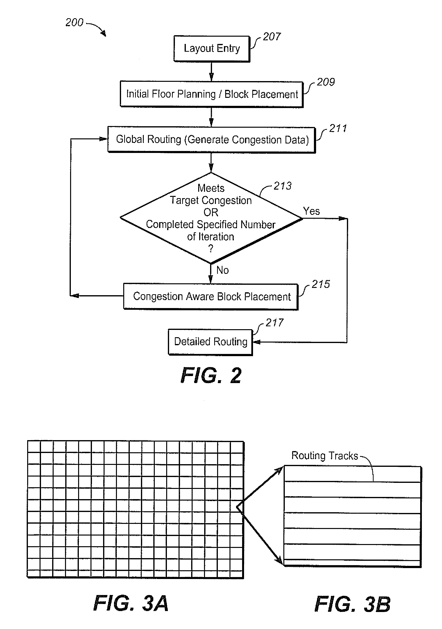
[0014]A circuit design process is presented that includes a block placement operation, followed by global routing based upon the initial placement of the blocks. Congestion data is generated from the global routing and, in an automated process, the blocks are placed again based upon the congestion data to reduce the routing congestion of the design.

Problems solved by technology

Routability of a design is determined by the routing congestion of the design, and decreases with the increase of routing congestion.
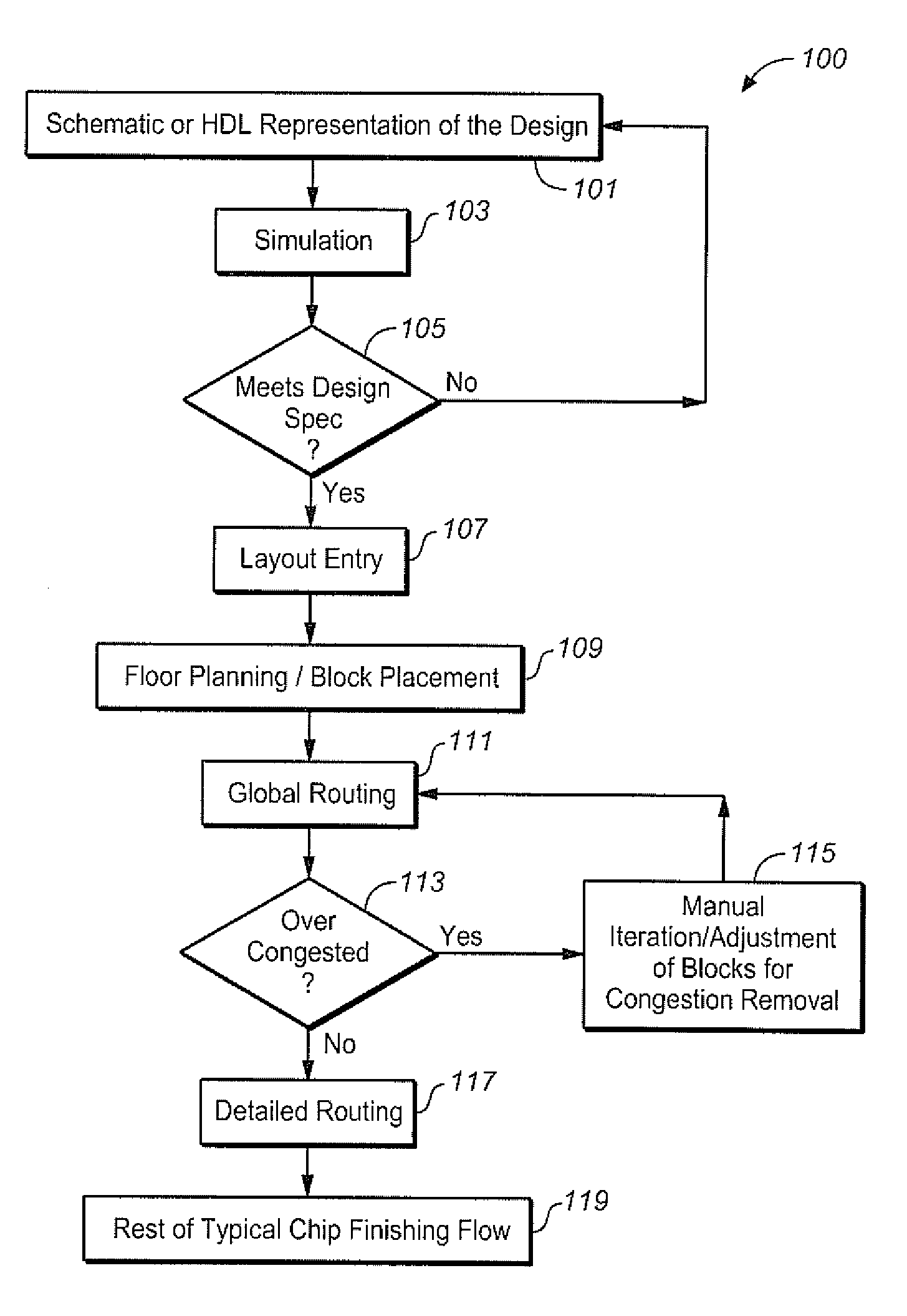
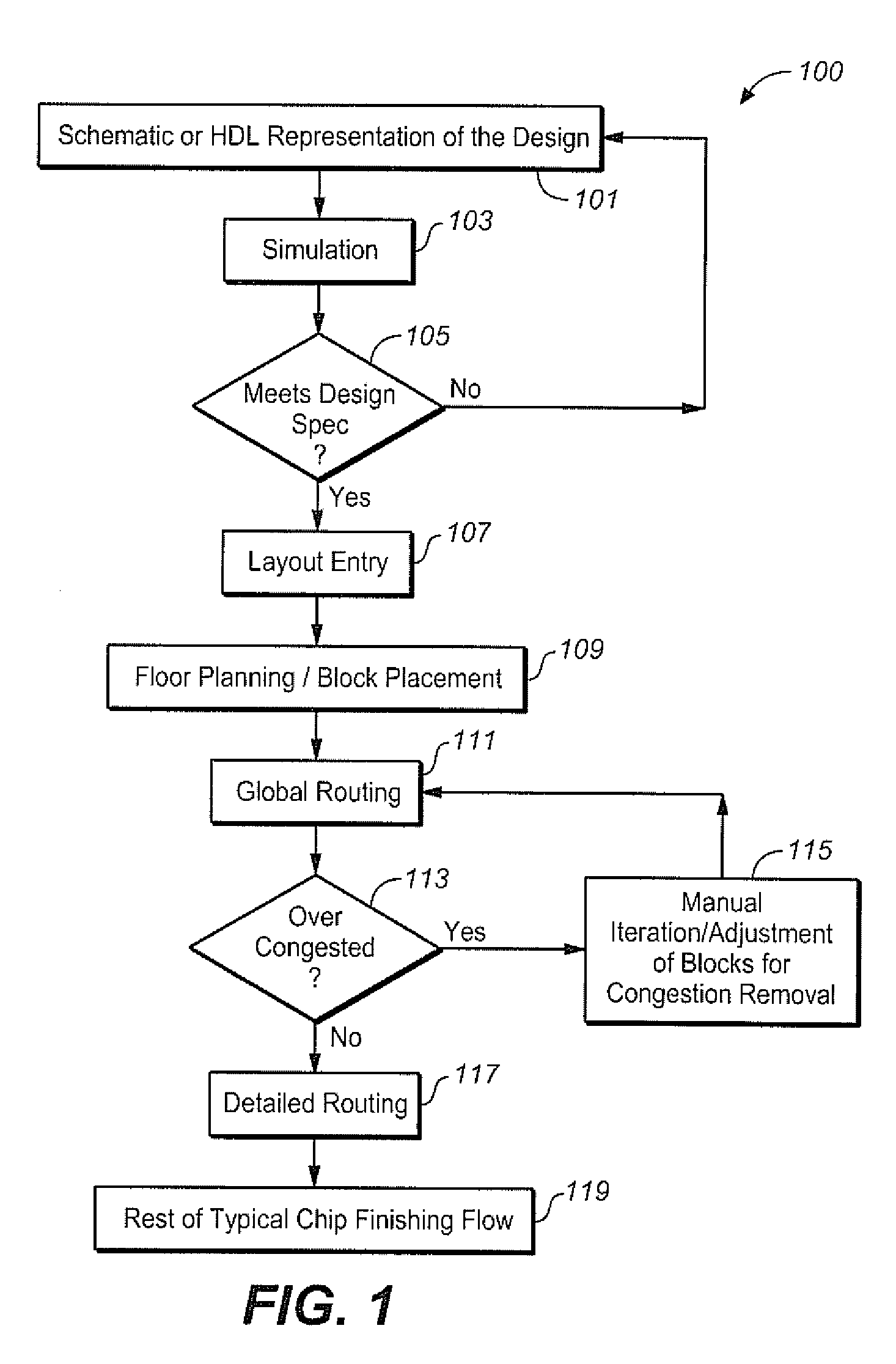
Manual iteration 115 is possible for a small design to reach a required congestion level, but for a big and / or complex mixed-signal design it is cumbersome or near impossible to do so.
Unlike the digital domain, spaces in custom domain are very irregular.
This increases the complexity in a custom block placer as it needs to search and optimize the entire design space.

Method used


Image

  • Congestion aware block placement
  • Congestion aware block placement
  • Congestion aware block placement

Examples


example embodiments

[0091]FIGS. 17-24 show screenshots of the display on a user's computer, that, along with the usual input devices (keyboard, mouse, etc.) serve as a user interface and represent how congestion is reduced in the design using embodiments of the present invention.

[0092]FIG. 17 shows an exemplary design with three blocks and FIG. 18 shows the congestion after global routing on the same design. In FIG. 18, the areas within the three ovals represent high congestion areas. FIG. 19 represents the modified placement using aspects of the present invention. As shown in FIG. 20, there is no congestion after global routing with the new placement.

[0093]FIG. 21 shows another design with six blocks. After the global routing (211, FIG. 2) it reports congestion at the bottom of the instance “top—1_port_receive”. A closer look at high congestion region (the oval 2101 just right of center at bottom of FIG. 21) is shown in the FIG. 22. FIG. 22 shows that there are three congested GCell in that region. Co...


PUM


Abstract

A circuit design process is presented that includes a block placement operation, followed by global routing based upon the initial placement of the blocks. Congestion data is generated from the global routing and, in an automated process, the blocks are placed again based upon the congestion data to reduce the routing congestion of the design. This can be used as part of a custom layout design process, for example.

Description

BACKGROUND OF THE INVENTION[0001]1. Field of Invention[0002]This invention relates to automated integrated circuit design data and, more specifically, to routing congestion removal during block placement, particularly for custom design.[0003]2. Description of Related Art[0004]A typical custom / analog design flow 100 is shown in FIG. 1 and starts with design entry 101; generally it is done through schematic entry or HDL representation. The design entry is done carefully to meet the design specification and is verified by simulation 103. When a design meets the required specification (“Yes”, 105) then its physical implementation starts which is known a physical design.[0005]Physical design can be broadly categorized into following stages:[0006]1. Layout Entry 107[0007]2. Floorplanning 109[0008]3. Routing[0009]Layout Entry 107 is the first step of physical design which is a physical representation of a design. At the floorplanning stage 109, the design is partitioned into various blocks...

Claims


Application Information

Patent Timeline
Patent Type & Authority Patents(United States)
IPC IPC(8): G06F17/50
CPCG06F17/5072G06F17/5077G06F30/394G06F30/392G06F30/3947
Inventor GHOSH, SANJIBGUPTA, VANDANAMARWAH, HITESHKHALSA, MAHENDRA SINGHFANGARIA, PAWAN
Owner CADENCE DESIGN SYST INC
Learn More