Method of forming semiconductor thin film and semiconductor thin film inspection apparatus

a technology of inspection apparatus and semiconductor, which is applied in the direction of individual semiconductor device testing, semiconductor/solid-state device testing/measurement, instruments, etc., can solve the problem of difficult monitoring of a fine difference in power density on the plane of inevitably arises a size or intensity of laser light applied to an object to be irradiated, and the effect of reliable screening

Inactive Publication Date: 2012-06-05
SONY CORP
View PDF6 Cites 2 Cited by
  • Summary
  • Abstract
  • Description
  • Claims
  • Application Information

AI Technical Summary

Benefits of technology

[0015]In the method of forming a semiconductor thin film according to the embodiment of the invention, after the amorphous semiconductor thin film is formed on the substrate, the laser light is applied to the amorphous semiconductor thin film to selectively perform the heating process on the amorphous semiconductor thin film, thereby the amorphous semiconductor thin film in the region irradiated with the laser light is crystallized thereby to form the crystalline semiconductor thin film partially in each element region. Then, after that, the crystallinity degree of the crystalline semiconductor thin film is inspected. In this case, in the step of inspecting, the contrast between the luminance of the crystallized region and the luminance of the non-crystallized region is determined by applying light to the crystalline semiconductor thin film and the amorphous semiconductor thin film, and screening of the crystalline semiconductor thin film is performed on the basis of the determined contrast. Thus, when screening of the crystalline semiconductor thin film is performed on the basis of the contrast between the luminance of the crystallized region and the luminance of the non-crystallized region, more reliable screening than ever before is achieved.
[0017]In the semiconductor thin film inspection apparatus according to the embodiment of the invention, on the substrate on which the crystalline semiconductor thin film is formed partially in each element region, light is applied from the light source to the crystalline semiconductor thin film and the amorphous semiconductor thin film. Then, on the basis of the light emitted from the light source, the contrast between the luminance of the crystallized region and the luminance of the non-crystallized region is determined, and on the basis of the determined contrast, screening of the crystalline semiconductor thin film is performed. Since screening of the crystalline semiconductor thin film is performed on the basis of the contrast between the luminance of the crystallized region and the luminance of the non-crystallized region, more reliable screening than ever before is achieved.
[0018]In the method of forming a semiconductor thin film according to the embodiment of the invention, in the step of inspecting the crystallinity degree of the crystalline semiconductor thin film, light is applied to the crystalline semiconductor thin film and the amorphous semiconductor thin film, thereby the contrast between the luminance of the crystallized region and the luminance of the non-crystallized region is determined, and screening of the crystalline semiconductor thin film is performed on the basis of the determined contrast, so more reliable screening than ever before is achieved. Therefore, when the semiconductor thin film is formed through the use of crystallization by laser annealing, the crystallinity degree is evaluated with higher precision than ever before.

Problems solved by technology

Moreover, even in the case where a uniform irradiation optical system is arranged to correct such an individual difference, an adjustment error or the like occurs.
Therefore, in the case where the annealing process is performed through the use of a plurality of laser beams, a difference in the size or intensity of laser light applied to an object to be irradiated arises inevitably.
Moreover, in the case of Japanese Unexamined Patent Application Publication No. 2005-101202, only the intensity (power) of a laser beam from each of laser light sources is monitored, so it is difficult to monitor a fine difference in power density on a plane of an object to be irradiated due to a focus position, aberration of an optical system or the like.
Such a difference in characteristics among the TFTs may cause display unevenness in a display.

Method used


Image

  • Method of forming semiconductor thin film and semiconductor thin film inspection apparatus
  • Method of forming semiconductor thin film and semiconductor thin film inspection apparatus
  • Method of forming semiconductor thin film and semiconductor thin film inspection apparatus

Examples


modification 1

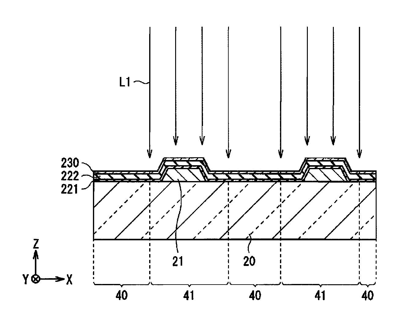
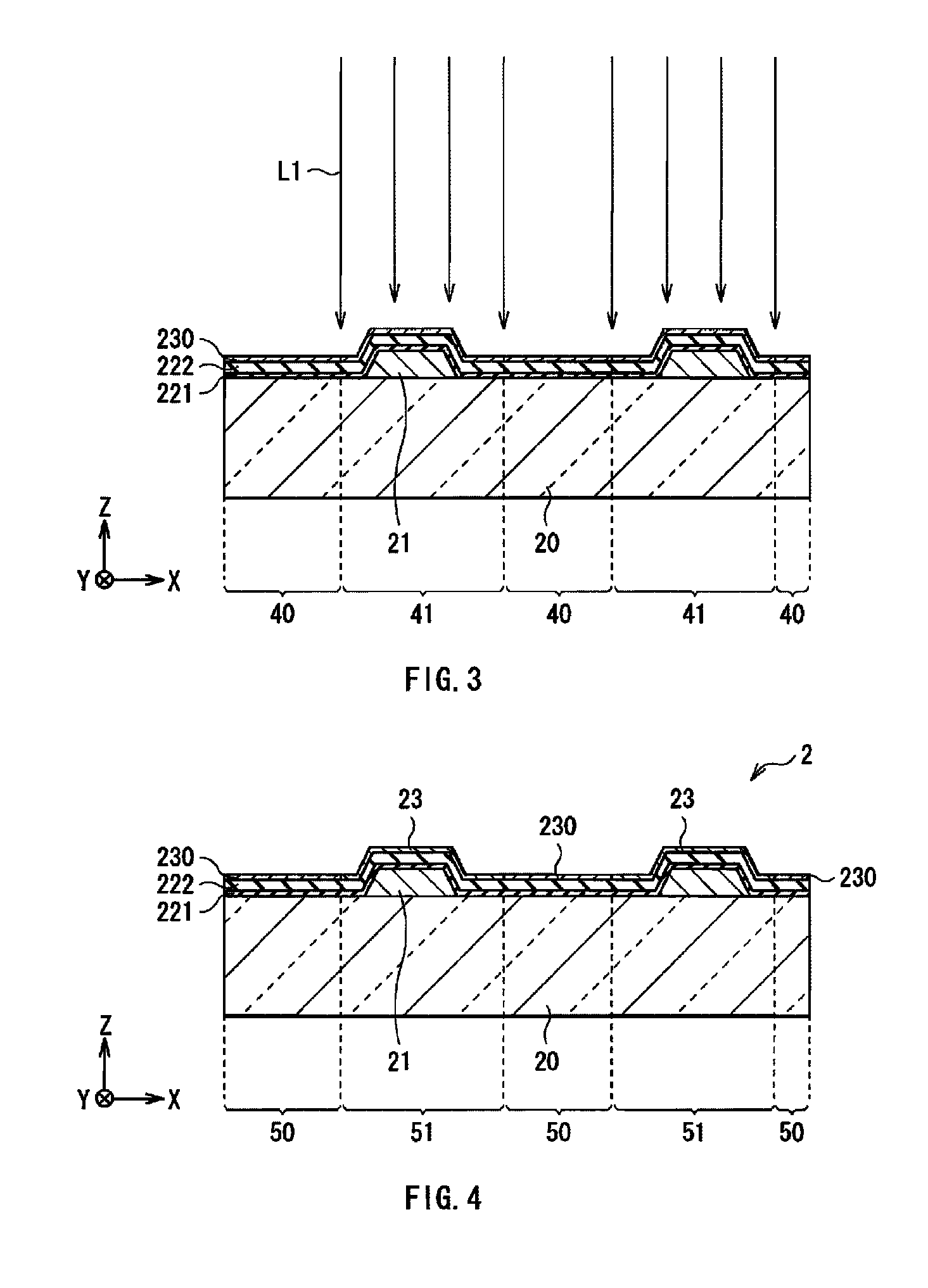
[0090]FIG. 12B is a sectional view (a Z-X sectional view) for describing an inspection process according to a modification 1. In the modification, the laser light L1 is applied to a light-absorbing layer 231 on the a-Si film 230 in a step of forming the p-Si film 23, thereby a heating process is performed indirectly on the a-Si film 230. In other words, in the above-described embodiment, for example, as illustrated in FIG. 12A, the laser light L1 is applied to the a-Si film 230 in the step of forming the p-Si film 23, thereby the heating process is performed directly on the a-Si film 230. On the other hand, in the modification, the heating process is performed indirectly on the a-Si film 230.

[0091]In the modification, measurement in a state in which the light-absorbing layer 231 is still laminated may be performed. In other words, transmittance shows a strong correlation between before and after the removal of the light-absorbing layer 231, so when a corresponding table is formed pr...

modification 9

[0101]FIGS. 21A and 21B are illustrations for describing an inspection step according to a modification 9, and FIG. 21A illustrates a plane configuration example of the Si thin film substrate 2 used in the inspection step in the modification, and FIG. 21B illustrates side configuration examples of the movable stage 11 and the Si thin film substrate 2 used in the inspection step in the modification.

[0102]As illustrated in FIGS. 21A and 21B, in the modification, a reference level measurement region 52 and a zero measurement region 53 are preliminarily arranged in predetermined positions on the Si thin film substrate 2 (the transparent substrate 20) (refer to FIG. 21A) or on the movable stage 11 on which the Si thin film substrate 2 is mounted (refer to FIG. 21B).

[0103]The reference level measurement region 52 is a measurement region for obtaining a reference image with respect to a picked-up image (the transmission image or the reflection image) on the basis of the irradiation light L...


PUM


Abstract

A method of forming a semiconductor thin film includes the steps of: forming an amorphous semiconductor thin film on a substrate; forming a crystalline semiconductor thin film partially in each element region by applying laser light to the amorphous semiconductor thin film to selectively perform a heating process on the amorphous semiconductor thin film, thereby crystallizing the amorphous semiconductor thin film in a region irradiated with the laser light; and inspecting the crystallinity degree of the crystalline semiconductor thin film. The step of inspecting includes the steps of determining a contrast between the luminance of a crystallized region and the luminance of a non-crystallized region by applying light to the crystalline semiconductor thin film and the amorphous semiconductor thin film, and performing screening of the crystalline semiconductor thin film on the basis of the determined contrast.

Description

BACKGROUND OF THE INVENTION[0001]1. Field of the Invention[0002]The present invention relates to a method of forming a semiconductor thin film suitable for manufacturing a TFT (Thin Film Transistor) substrate used in, for example, a liquid crystal display or an organic EL (ElectroLuminescence) display, and an inspection apparatus for such a semiconductor thin film.[0003]2. Description of the Related Art[0004]In an active matrix liquid crystal display or an organic EL display using an organic EL device, a TFT substrate is used. The TFT substrate is formed by forming a an amorphous semiconductor thin film or a polycrystalline semiconductor thin film with a relatively small particle diameter on a substrate, and forming a TFT as a drive element through the use of a semiconductor thin film crystal grown by annealing the amorphous semiconductor thin film or the polycrystalline semiconductor thin film by irradiation with a laser beam.[0005]As a light source of an annealing apparatus using ...

Claims


Application Information

Patent Timeline
Patent Type & Authority Patents(United States)
IPC IPC(8): H01L21/66
CPCG01N21/956H01L27/1285H01L22/12H01L29/66765H01L29/78678G01N2021/9513H01L21/02532H01L21/02675
Inventor UMEZU, NOBUHIKOTSUKIHARA, KOICHIAMAGO, HIROHISAMATSUNOBU, GOSHIRAI, KATSUYA
Owner SONY CORP
Why Eureka
Try Eureka