Liquid crystal display device and its manufacture method

a liquid crystal display and manufacturing method technology, applied in non-linear optics, instruments, optics, etc., can solve the problems of alignment defect formation and damage to the liquid crystal alignment function of the alignment film, and achieve the effect of removing alignment defects

Active Publication Date: 2012-05-15
STANLEY ELECTRIC CO LTD
View PDF8 Cites 0 Cited by
  • Summary
  • Abstract
  • Description
  • Claims
  • Application Information

AI Technical Summary

Benefits of technology

[0008]It is an object of the present invention to provide a liquid crystal display device capable of eliminating alignment defects to be caused by static electricity generated during a rubbing process, and its manufacture method.

Problems solved by technology

As this static electricity is discharged, a liquid crystal alignment function of the alignment film is damaged and an alignment defect is formed.

Method used


Image

  • Liquid crystal display device and its manufacture method
  • Liquid crystal display device and its manufacture method
  • Liquid crystal display device and its manufacture method

Examples


Embodiment Construction

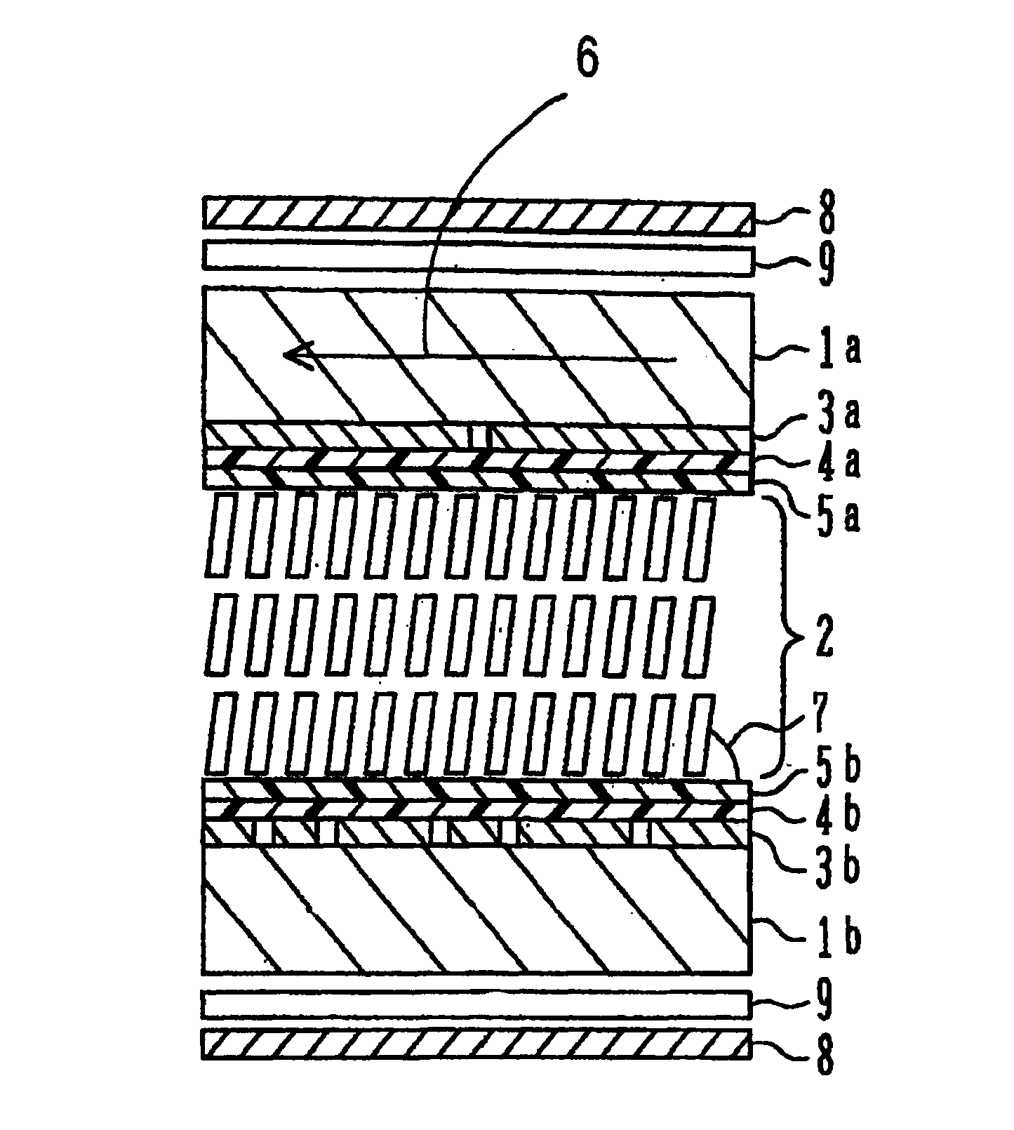
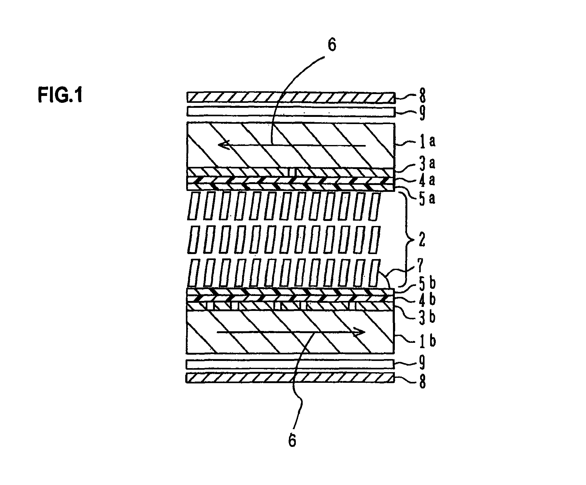
[0018]FIG. 1 is a schematic cross sectional view of a liquid crystal display device used for an embodiment and experiments. The liquid crystal display device shown has a transparent upper substrate 1a and an opposing transparent lower substrate 1b, and a liquid crystal layer 2. A device outer size is a lateral length of about 160 mm and a vertical length of about 50 mm. A transparent upper electrode 3a is formed as a common electrode on the upper substrate 1a on the liquid crystal layer 2 side. A transparent lower electrode 3b is formed as a segment electrode on the lower substrate 1b. Both the transparent electrodes 3a and 3b are superposed upon each other, sandwiching the liquid crystal layer 2. The superposed area defines a display area. Both the substrates 1a and 1b are provided with alignment films 5a and 5b on the liquid crystal layer 2 side, the alignment films covering both the transparent electrodes. Insulating films 4a and 4b are formed between the alignment films 5a and 5...


PUM

PropertyMeasurementUnit
surface free energyaaaaaaaaaa
angleaaaaaaaaaa
vertical lengthaaaaaaaaaa

Abstract

A liquid crystal display device using a low duty ratio driving method with a duty ratio not smaller than 1 / 16 is manufactured in the following manner. A first substrate is prepared having a first electrode of a predetermined shape. A second substrate is prepared having a second electrode of a shape different from said predetermined shape, the second electrode having signal line electrodes smaller in number than those of the first electrode. An insulating film having necessary insulation is formed on each of the first and second electrodes. First and second vertical alignment films are formed above the first and second substrates, respectively, the first and second vertical alignment films covering the first and second electrodes, respectively. A rubbing process is executed only for the second vertical alignment film. The first and second substrates are disposed facing each other, and liquid crystal having a negative dielectric constant anisotropy is disposed between the first and second substrates. It is possible to prevent alignment defects to be caused by static electricity generated by rubbing of a liquid crystal display device.

Description

CROSS REFERENCE TO RELATED APPLICATION[0001]This application is based on and claims priority of Japanese Patent Application No. 2007-014580 filed on Jan. 25, 2007, the entire contents of which are incorporated herein by reference.BACKGROUND OF THE INVENTION[0002]A) Field of the Invention[0003]The present invention relates to a liquid crystal display device and its manufacture method, and more particularly to a vertical alignment type liquid crystal display device and its manufacture method.[0004]B) Description of the Related Art[0005]Alignment directions of liquid crystal molecules of a liquid crystal display device (particularly a vertical alignment type liquid crystal display device) are controlled by a rubbing process for alignment films to improve the image quality. The present inventors and others have proposed in JP-A-2005-234254 a liquid crystal display device having a uniform pretilt angle and no rubbing flaws after a rubbing process for an organic polymer material thin film...

Claims


Application Information

Patent Timeline
Patent Type & Authority Patents(United States)
IPC IPC(8): G02F1/1337
CPCG02F1/1393G02F1/133784G02F1/134327
Inventor IWAMOTO, YOSHIHISASHIMIZU, HAJIME
Owner STANLEY ELECTRIC CO LTD
Why Eureka
Try Eureka