Failure detecting method, failure detecting apparatus, and semiconductor device manufacturing method

a failure detection and manufacturing method technology, applied in the direction of total factory control, programme control, electric controllers, etc., can solve the problems of unbalance somewhere, difficult to identify the cause of lsi failure, and yield declin

Active Publication Date: 2012-05-01
KIOXIA CORP
View PDF10 Cites 3 Cited by
  • Summary
  • Abstract
  • Description
  • Claims
  • Application Information

AI Technical Summary

Problems solved by technology

However, since an LSI is produced through several hundred steps and manufacturing apparatuses, identifying the cause of LSI failures is very difficult work.
Failure distribution in the wafer surface is largely divided into two types, random failures evenly distributed without depending on the position on the wafer surface, and clustering failures causing unbalance somewhere.
Among these, for the clustering failures, the factor of the clustering failures is often due to a process, a manufacturing apparatus, and the like, and the clustering failures are a great cause of yield decrease.
It is indicated that failures caused by a process and a manufacturing apparatus leave “a fingerprint” as failure distribution on the wafer surface.
In other words, if a problem occurs in a certain process and manufacturing apparatus, clustering failures specific to the process and manufacturing apparatus occur.
However, since not all chips corresponding to the places where a defect is present are failed, it is difficult to identify the processing process that is the cause of failure occurrence by comparison of the predicted probe inspection map and the probe inspection map.

Method used


Image

  • Failure detecting method, failure detecting apparatus, and semiconductor device manufacturing method
  • Failure detecting method, failure detecting apparatus, and semiconductor device manufacturing method
  • Failure detecting method, failure detecting apparatus, and semiconductor device manufacturing method

Examples


Embodiment Construction

[0051]An embodiment of the present invention will be described below with reference to the drawings.

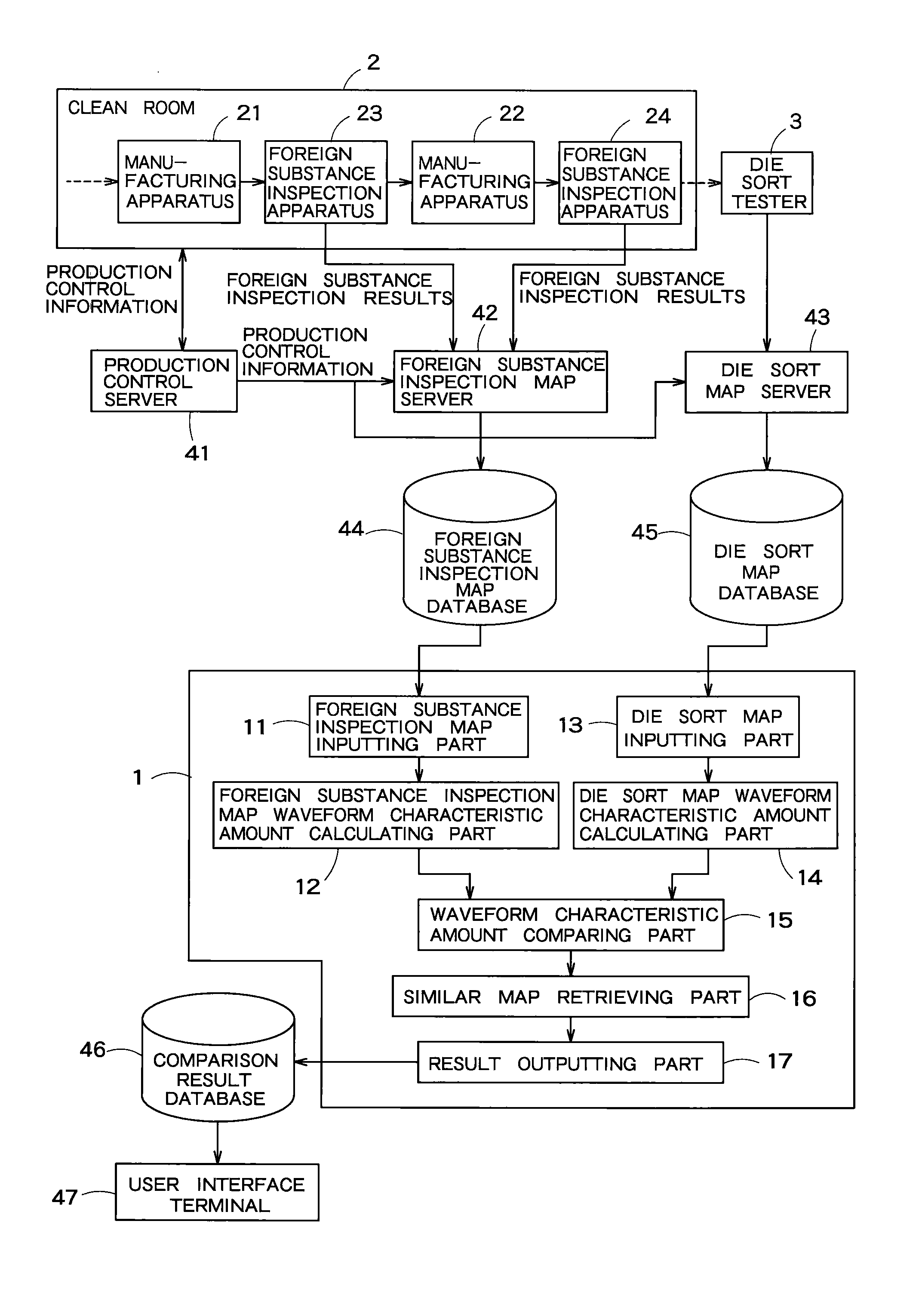
[0052]A schematic configuration of a semiconductor manufacturing system including a failure detecting apparatus 1 according to the embodiment of the present invention is shown in FIG. 1. The inspection of a wafer surface is performed by foreign substance inspecting apparatuses 23 and 24 after wafer processing processes performed by manufacturing apparatuses 21 and 22 in a clean room 2. This inspection is performed optically or with an electron beam, and foreign substances, such as dust and electrical wiring pattern abnormality, are detected.

[0053]As a result of the inspection, foreign substance inspection maps in which the locations of foreign substances are mapped and displayed on a wafer surface are created, and stored in a foreign substance inspection map database 44 via a foreign substance inspection map server 42. For example, a foreign substance inspection map as shown in FIG. 2...


PUM


Abstract

A method for inputting a foreign substance inspection map created by foreign substance inspection for a wafer surface after each processing process in a wafer processing process, inputting a die sort map created by a die sort test after the wafer processing process, setting region segments in the wafer, setting a region number for each segment, calculating foreign substance density of the region segments, based on the foreign substance inspection map, and plotting the foreign substance density, using the region numbers, to calculate a foreign substance inspection map waveform characteristic amount, calculating failure density in the region segments, based on the die sort map, and plotting the failure density, using the region numbers, to calculate a die sort map waveform characteristic amount, calculating similarity between the foreign substance inspection map waveform characteristic amount and the die sort map waveform characteristic amount, and identifying a processing process cause of failure occurrence.

Description

CROSS REFERENCE TO RELATED APPLICATION[0001]This application is based upon and claims benefit of priority from the Japanese Patent Application No. 2007-281490, filed on Oct. 30, 2007, the entire contents of which are incorporated herein by reference.BACKGROUND OF THE INVENTION[0002]The present invention relates to a failure detecting method, a failure detecting apparatus, and a semiconductor device manufacturing method.[0003]In order to improve the yield of LSI manufacturing, it is important to analyze the yield loss, early clarify the process, manufacturing apparatus, or design condition that is the cause of the yield loss, and improve it. However, since an LSI is produced through several hundred steps and manufacturing apparatuses, identifying the cause of LSI failures is very difficult work.[0004]For the clarification of the cause of failures, the results of an electrical property test (a die sort test) that is performed after the wafer process is finished may be used. The die so...

Claims


Application Information

Patent Timeline
Patent Type & Authority Patents(United States)
IPC IPC(8): G06F19/00
CPCG05B19/41875G05B23/0229G05B2219/11G05B2219/1112G05B2219/32222G05B2219/45031G05B2223/02Y02P90/02
Inventor MATSUSHITA, HIROSHIKADOTA, KENICHIARITAKE, TOSHIYUKI
Owner KIOXIA CORP
Why Eureka
Try Eureka