
Object placement in integrated circuit design

a technology of integrated circuits and objects, applied in the field of data processing systems, can solve problems such as complex designs produced and manipulated using software tools, and achieve the effect of reducing congestion and reducing pin density in the area

Active Publication Date: 2012-01-31
SIEMENS PROD LIFECYCLE MANAGEMENT SOFTWARE INC
View PDF15 Cites 6 Cited by
  • Summary
  • Abstract
  • Description
  • Claims
  • Application Information

AI Technical Summary

Benefits of technology

The patent describes a method, system, and computer program for improving the placement of objects in integrated circuit design. It involves estimating the initial placement of the objects, transforming the placement to improve certain characteristics, such as congestion or pin density, and re-estimating the transformed placement to determine if it has improved. The final placement is then produced based on the improved characteristic. The transformation may include resizing, weighting, clustering, shortening routes, or straightening bends, among others. The technical effects of this patent include improved global and detailed routing, reduced congestion, and reduced pin density.

Problems solved by technology

The designs produced and manipulated using these software tools are complex, often including hundreds of thousands of such components interconnected to form an intended electronic circuitry.

Method used


Image

  • Object placement in integrated circuit design
  • Object placement in integrated circuit design
  • Object placement in integrated circuit design

Examples


Embodiment Construction

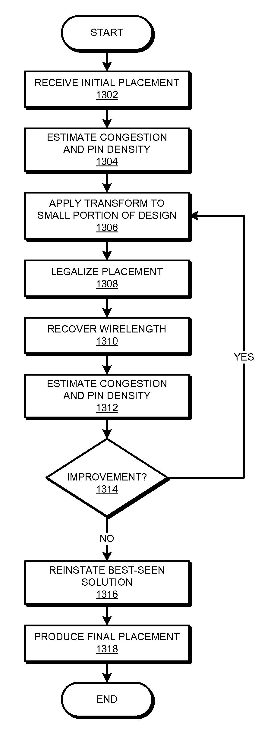
[0032]In a portion of the IC design process, IC design tools generally employ various steps in producing an IC design that works as intended. A circuit designer generally creates the design in a computer programming language in the form of code. The IC design tool accepts the design in the code form and generates a rendering of the design in multiple layers that have be formed in a semiconducting material to create a circuit according to that design.

[0033]The IC design tool identifies cells in the design. The IC design tool manipulates a set of the cells to legalize the design. A set of cells is one or more cells. Legalizing the design is manipulating the cells so no cells overlap each other in the rendering or when formed in the semiconducting material. A legal design results from the legalizing operation. Cells are generally allowed to touch other cells but not overlap in a legal design.

[0034]A type of cell in an IC design is known as a standard cell. A standard cell is combinatio...


PUM


Abstract

A method, system, and computer usable program product for an improved object placement in integrated circuit design are provided in the illustrative embodiments. The IC design includes cells, the cells including electronic components, wires, and pins defined for interconnections of the IC. An initial placement corresponding to the design is received. A characteristic of the initial placement is estimated, which may include congestion, pin density, or both in an area of the initial placement. A transformation is performed on a part of the initial placement including the area to improve the characteristic. If the characteristic has improved in the transformed placement, a final placement corresponding to the transformed placement is produced. The transformation may be any combination of resizing an object, weighting a connection, clustering a plurality of objects, shortening of a route taken by a wire, and straightening a bend in a wire in the initial placement.

Description

BACKGROUND OF THE INVENTION[0001]1. Field of the Invention[0002]The present invention relates generally to an improved data processing system, and in particular, to a computer implemented method for integrated circuit design. Still more particularly, the present invention relates to a computer implemented method, system, and computer usable program code for improved object placement in integrated circuit (IC) design.[0003]2. Description of the Related Art[0004]Modern day electronics include components that use integrated circuits. Integrated circuits are electronic circuits formed using Silicon as a substrate and by adding impurities to form solid-state electronic devices, such as transistors, diodes, and resistors. Commonly known as a “chip”, an integrated circuit is generally encased in hard plastic. The components in modern day electronics generally appear to be rectangular black plastic pellets with connector pins protruding from the plastic encasement.[0005]Circuit designers us...

Claims


Application Information

Patent Timeline
Patent Type & Authority Patents(United States)
IPC IPC(8): G06F17/50
CPCG06F17/5072G06F2217/08G06F2111/06G06F30/392
Inventor ALPERT, CHARLES JAYNAM, GI-JOONROY, JARROD ALEXANDERVISHVANATHAN, NATARAJAN
Owner SIEMENS PROD LIFECYCLE MANAGEMENT SOFTWARE INC
Learn More