Display device and method for manufacturing display device
a technology of display device and display device, which is applied in the field of display device, can solve the problems of long time required for forming inorganic film and etching process, large inapplicability, and achieves the effect of reducing the cost of vacuum apparatus, high material use efficiency, and low cos
- Summary
- Abstract
- Description
- Claims
- Application Information
AI Technical Summary
Benefits of technology
Problems solved by technology
Method used
Image

Examples
embodiment mode 1
This embodiment mode will describe an example of a function layer in a display device aimed at higher image quality and higher reliability, which can be manufactured at low cost with high productivity.
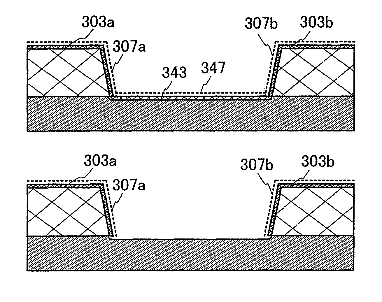
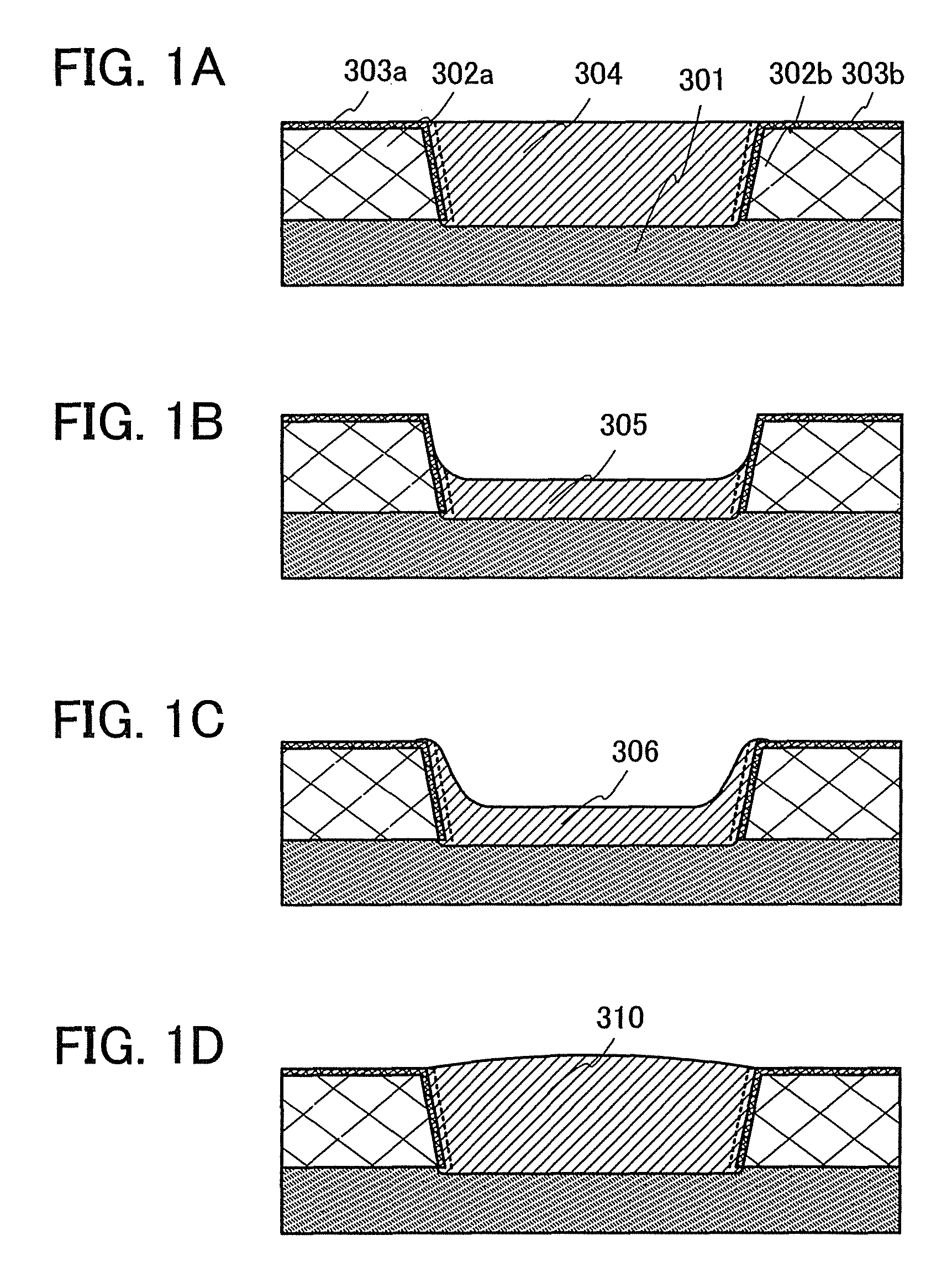
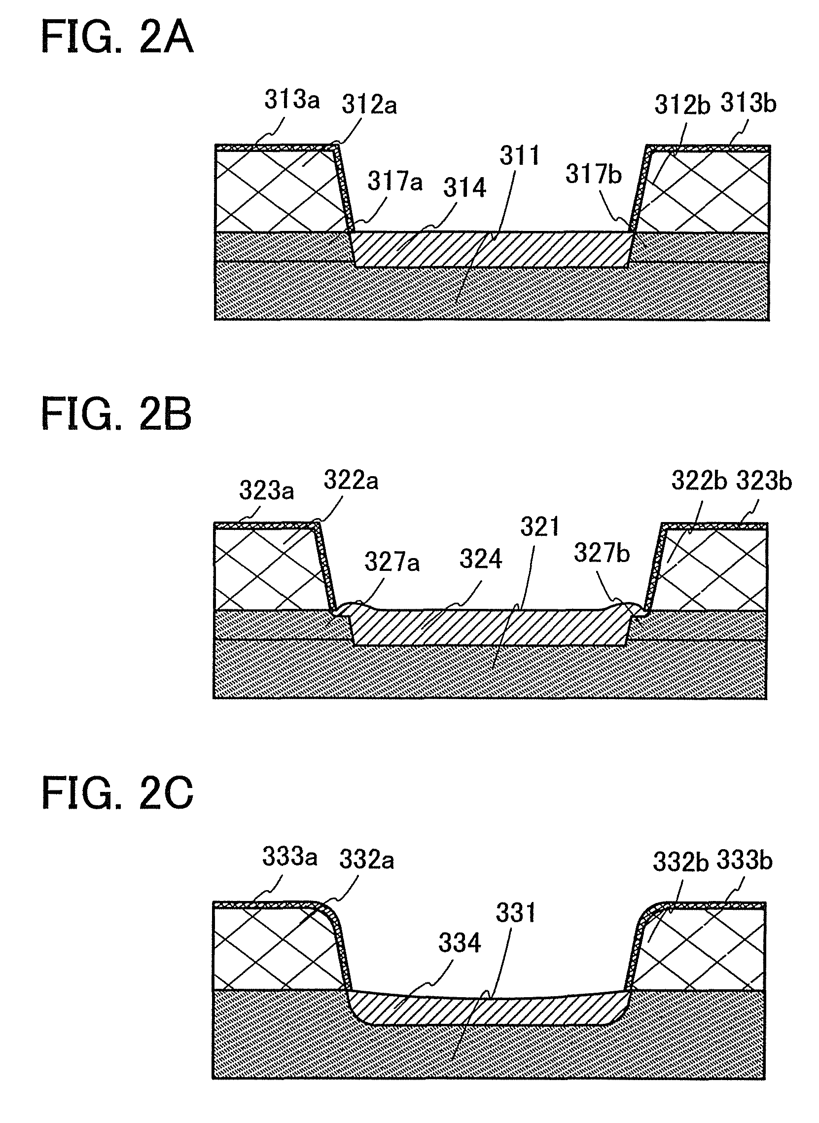
FIGS. 1A to 1D and FIGS. 2A to 2C show an example of a function layer of the present invention. FIG. 1A shows an example in which in an opening formed with a layer 301 including an organic compound (a first organic compound) and layers 302a and 302b including an organic compound (a second organic compound), a function layer 304 is formed so that the opening can be filled with the function layer 304. Oxide layers 303a and 303b are formed on surfaces of the layers 302a and 302b including an organic compound to be interposed between the function layer 304 and the layers 302a and 302b. The layer 301 including an organic compound at a base of the opening is a region with the small thickness and a depressed portion is formed because an oxide layer formed on a surface of the layer 301 by oxid...
embodiment mode 2
This embodiment mode will describe an example of a display device aimed at higher image quality and higher reliability, which can be manufactured at low cost with high productivity. More specifically, a passive matrix display device is shown.
FIGS. 4A and 4B each show a passive matrix liquid crystal display device to which the present invention is applied. FIG. 4A illustrates a reflective liquid crystal display device and FIG. 4B illustrates a transmissive liquid crystal display device. In FIGS. 4A and 4B, a substrate 1700 and a substrate 1710 are provided opposite to each other with a liquid crystal layer 1703 interposed therebetween. The substrate 1700 is provided with electrode layers 1701a, 1701b, and 1701c also referred to as pixel electrode layers, which are used for display elements 1713 and an insulating layer 1712 serving as an alignment film, coloring layers 1706a, 1706b, and 1706c serving as part of a color filter, a layer 1720 including an organic compound, a layer 1723 i...
embodiment mode 3
This embodiment mode will describe an example of a display device aimed at higher image quality and higher reliability, which can be manufactured at low cost with high productivity. Specifically, this embodiment mode illustrates a liquid crystal display device that uses liquid crystal elements as display elements. Note that, this embodiment mode describes an active matrix liquid crystal display device, which is different from Embodiment Mode 2.
FIG. 8A is a top view of a liquid crystal display device which is one mode of the present invention. FIG. 8B is a cross-sectional view taken along a line C-D in FIG. 8A.
As shown in FIG. 8A, a pixel region 606 and driver circuit regions 608a and 608b which are scan line driver circuits are sealed between a substrate 600 and a counter substrate 695 with a sealing material 692. In addition, a driver circuit region 607 which is a signal line driver circuit including a driver IC is provided over the substrate 600. In the pixel region 606, a transis...
PUM
| Property | Measurement | Unit |
|---|---|---|
| temperature | aaaaa | aaaaa |
| temperature | aaaaa | aaaaa |
| light transmittance | aaaaa | aaaaa |
Abstract
Description
Claims
Application Information
 - R&D
- Intellectual Property
- Life Sciences
- Materials
- Tech Scout
- Unparalleled Data Quality
- Higher Quality Content
- 60% Fewer Hallucinations
Browse by: Latest US Patents, China's latest patents, Technical Efficacy Thesaurus, Application Domain, Technology Topic, Popular Technical Reports.
© 2025 PatSnap. All rights reserved.Legal|Privacy policy|Modern Slavery Act Transparency Statement|Sitemap|About US| Contact US: help@patsnap.com