Level-shift circuit
a level-shift circuit and circuit technology, applied in logic circuits, logic circuit coupling arrangements, pulse techniques, etc., can solve problems such as unreliable signal transmission to the high-side switch, and achieve the effect of preventing unreliable signal transmission and reliable signal transmission
- Summary
- Abstract
- Description
- Claims
- Application Information
AI Technical Summary
Benefits of technology
Problems solved by technology
Method used
Image
Examples
first exemplary embodiment
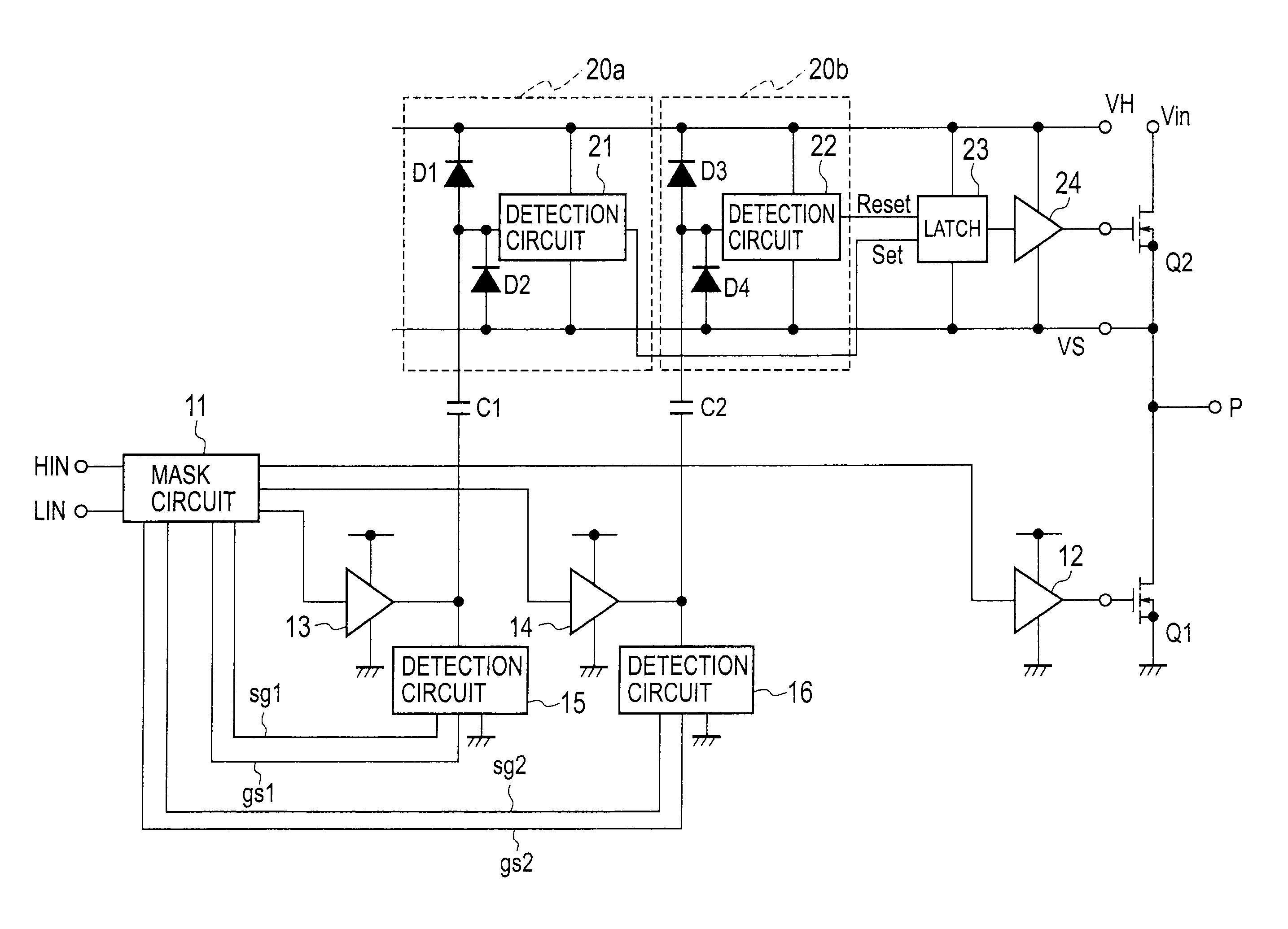
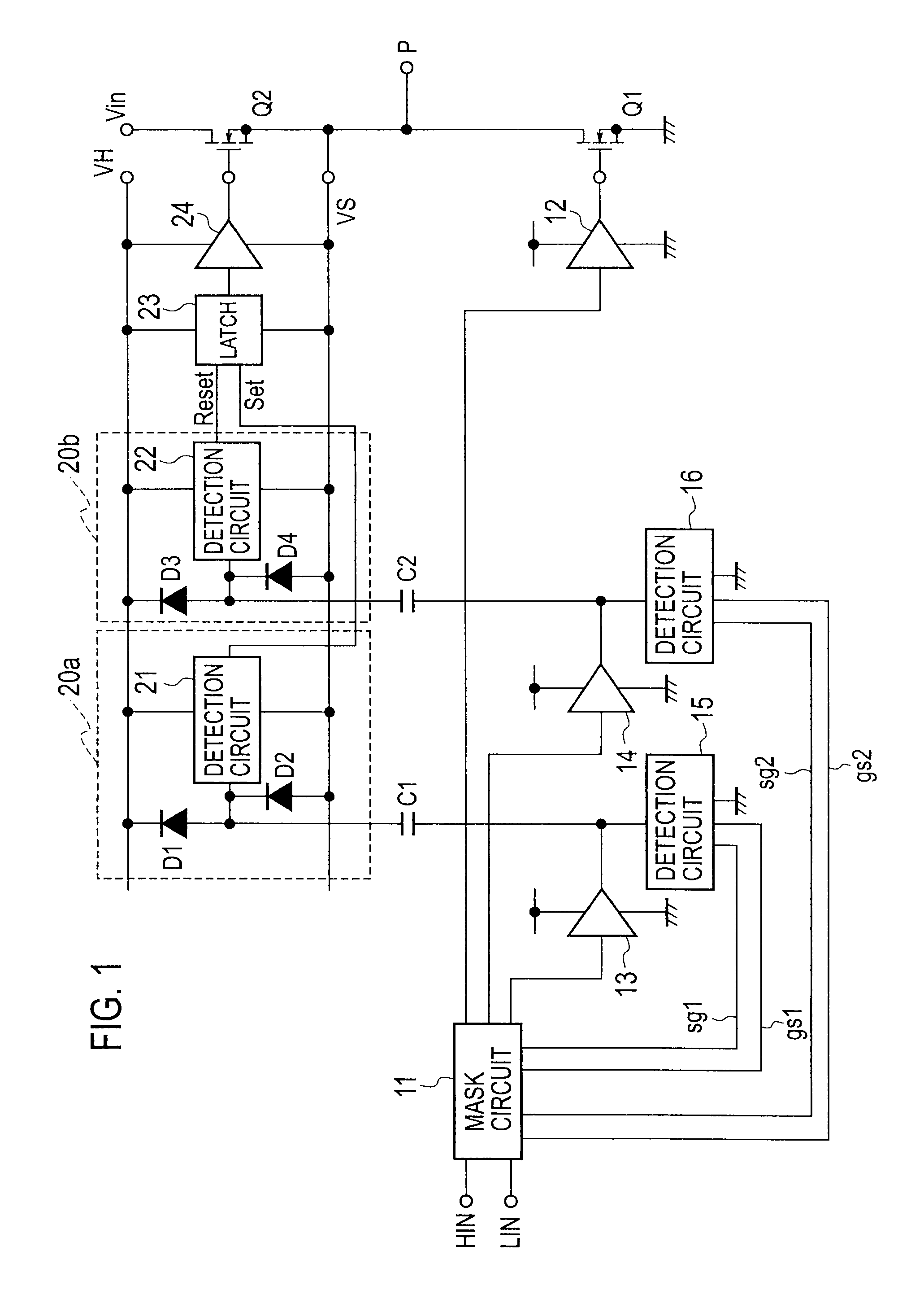
FIG. 1 is a block diagram illustrating a level-shift circuit according to a first exemplary embodiment of the present invention. In the level-shift circuit, a series circuit is connected between a power source Vin and the ground. In the series circuit, a low-side switch Q1 composed of MOSFET is connected to a high-side switch Q2 composed of MOSFET in series. The low-side switch Q1 and the high-side switch Q2 make up a half-bridge circuit.
It is noted that instead of the half-bridge circuit, a full-bridge circuit may be employed.
A mask circuit 11 outputs to a drive circuit 12 a low-side instruction signal input into a LIN terminal thereof. The drive circuit 12 drives the low-side switch Q1 based on the low-side instruction signal from the mask circuit 11.
The mask circuit 11 outputs to buffers 13 and 14 a high-side instruction signal input into a HIN terminal thereof. A first capacitor C1 is connected to an output of the buffer 13. The buffer 13 sends a set signal to a first high-side ...
second exemplary embodiment
FIG. 6 is a block diagram illustrating a level-shift circuit according to a second exemplary embodiment of the present invention. The level-shift circuit shown in FIG. 6 differs from the level-shift circuit shown in FIG. 1 in that a detection circuit 17, a third capacitor C3, diodes D5 and D6 and a buffer 18 are added and a signal detection method of detection circuits 21a and 22a in the detection circuits 15a and 16a is changed in a differential manner.
A series circuit composed of the diodes D5 and D6 is connected between the high potential VH and the high-side ground potential VS. A connection point of the diodes D5 and D6 is connected to the detection circuit 21a of a first high-side signal detection circuit 20c and the detection circuit 22a of a second high-side signal detection circuit 20d and connected to the detection circuit 17 and the buffer 18 via the third capacitor C3.
The detection circuit 17 detects a charging current flowing into the third capacitor C3 or a discharging...
PUM
 Abstract
Description
Claims
Application Information
 - R&D
- Intellectual Property
- Life Sciences
- Materials
- Tech Scout
- Unparalleled Data Quality
- Higher Quality Content
- 60% Fewer Hallucinations
Browse by: Latest US Patents, China's latest patents, Technical Efficacy Thesaurus, Application Domain, Technology Topic, Popular Technical Reports.
© 2025 PatSnap. All rights reserved.Legal|Privacy policy|Modern Slavery Act Transparency Statement|Sitemap|About US| Contact US: help@patsnap.com


