Circuit board based connector with raised projection section
a technology of circuit board and connector, applied in the direction of cross-talk/noise/interference reduction, connection contact member material, coupling device connection, etc., can solve the problems of inability to meet the needs of users, high mold cost, complicated structure of conventional connectors equipped with additional retention structures, etc., to reduce the manufacturing cost of plug-type connectors and small size
- Summary
- Abstract
- Description
- Claims
- Application Information
AI Technical Summary
Benefits of technology
Problems solved by technology
Method used
Image
Examples
first embodiment
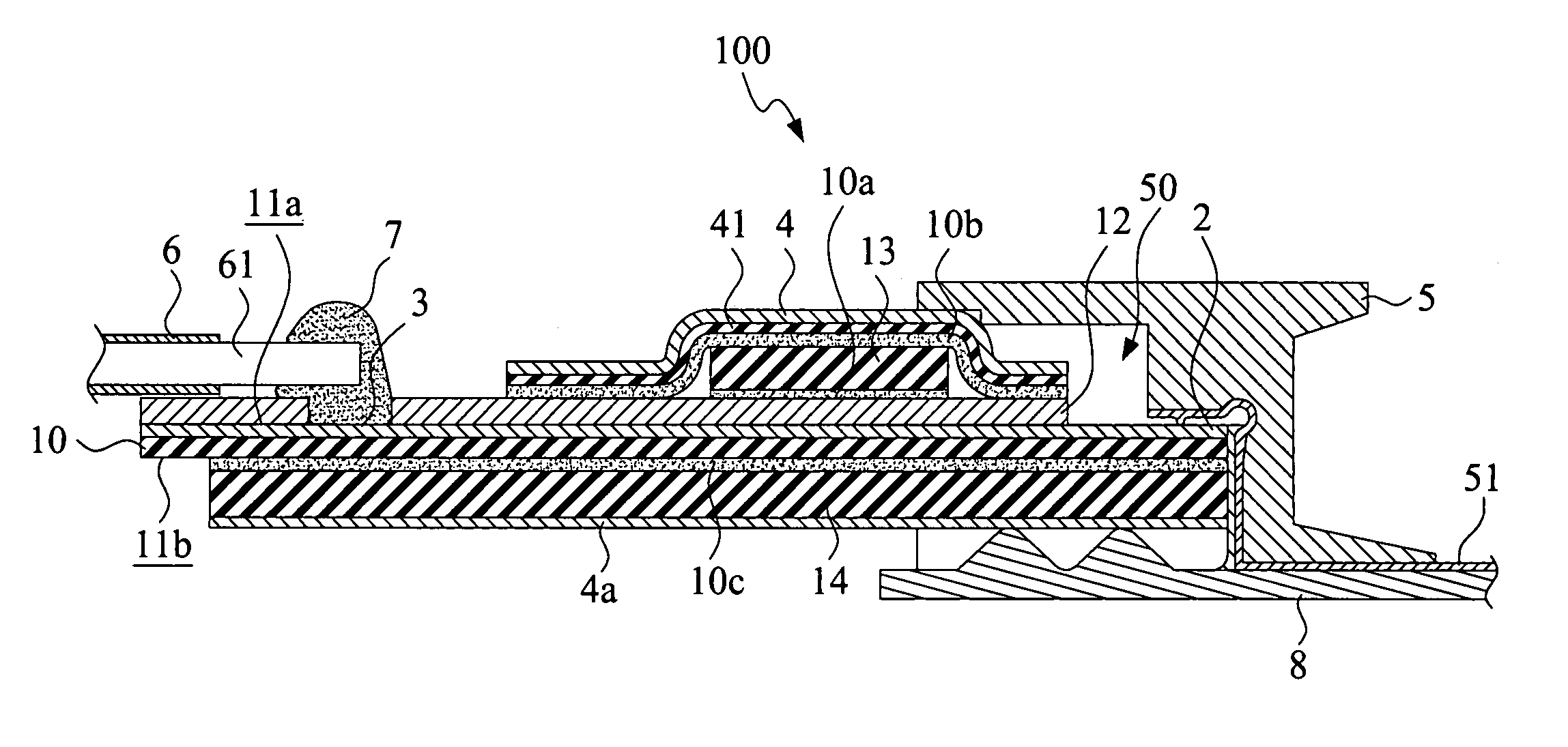
[0027]With reference to the drawings and in particular to FIGS. 1 and 2, of which FIG. 1 shows a perspective view of a first embodiment in accordance with the present invention and FIG. 2 shows a cross-sectional view taken along line 2-2 of FIG. 1, the present invention provides an circuit board based connector with raised projection section, generally designated at 100. The circuit board based connector 100 comprises a circuit substrate 1. The circuit substrate 1 has a first surface 11a and a second surface 11b. An end of the circuit substrate 1 is provided with a plurality of spaced conductive terminals 2. The circuit substrate 1 also has an end opposite to the conductive terminals 2 and provided with a plurality of spaced flat cable connection terminals 3.
[0028]The circuit substrate 1 is covered with an insulation layer 12. Bonded atop the insulation layer 12 with an adhesive layer 10a is at least one projection section 13, which is raised above a reference datum plane defined by...
fourth embodiment
[0038]The first shielding layer 4 and the fourth shielding layer 4c are connected to each other through a via 11e and solder 44 and are also in electrical connection with a grounding pattern 31 preset in the circuit substrate 1, or are connected through a via 11f that carries a conductive substance 45 (see FIG. 9 that shows a cross-sectional view of a circuit board based connector 100d in accordance with the present invention) and also in electrical connection with a grounding pattern 32 preset in the circuit substrate 1.
fifth embodiment
[0039]FIG. 10 is a cross-sectional view of a fifth embodiment in accordance with the present invention. The embodiment provides a circuit board based connector 100e that is applicable to a double-sided circuit substrate. Namely, the second surface 11b of the circuit substrate 1 has an undersurface that forms a conductive layer 18 and an insulation layer 12a. The insulation layer 12a has an undersurface that is bonded to a substrate 14b with an adhesive layer 10g and a fourth shielding layer 4c is formed on an undersurface of the substrate 14b. In this embodiment, the insulation layer 12a does not completely covers or overlaps the whole conductive layer 18 and at least one flat cable connection terminal 18a is formed on the undersurface of the conductive layer 18 at a selected location.
[0040]To connect flat cables to the connector 100e, the conductive terminals of a flat cable can be bonded to the flat cable connection terminals 3 with solders, or the conductive terminals of another ...
PUM
 Abstract
Description
Claims
Application Information
 - R&D
- Intellectual Property
- Life Sciences
- Materials
- Tech Scout
- Unparalleled Data Quality
- Higher Quality Content
- 60% Fewer Hallucinations
Browse by: Latest US Patents, China's latest patents, Technical Efficacy Thesaurus, Application Domain, Technology Topic, Popular Technical Reports.
© 2025 PatSnap. All rights reserved.Legal|Privacy policy|Modern Slavery Act Transparency Statement|Sitemap|About US| Contact US: help@patsnap.com


