Film bulk acoustic wave resonator, its fabrication method and film bulk acoustic wave resonator filter using the resonator
a technology of acoustic wave resonator and a fabrication method, which is applied in the direction of piezoelectric/electrostrictive transducers, generators/motors, transducer types, etc., can solve the problems of difficult to obtain good resonance characteristics, and difficult to completely trap a bulk acoustic wave inside the resonator, so as to reduce the connection between th
- Summary
- Abstract
- Description
- Claims
- Application Information
AI Technical Summary
Benefits of technology
Problems solved by technology
Method used
Image
Examples
embodiment 1
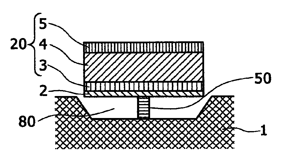
[0034]FIG. 1A is a top schematic view of a film bulk acoustic wave resonator according to a first embodiment, and FIGS. 1B and 1C each show a cross-sectional schematic view of the film bulk acoustic wave resonator according to the first embodiment. In detail, the FIG. 1B is a sectional view taken along line A-A in FIG. 1A, and FIG. 1C is a sectional view taken along line B-B in FIG. 1A. An FBAR-type film bulk acoustic wave resonator is formed on an insulating substrate 1. A laminate-structured resonance part 20 of this FBAR-type film bulk acoustic wave resonator has a laminate structure including a piezoelectric layer 4, and a pair of electrode layers (a first electrode layer 3 and a second electrode layer 5) interposing at least part of the piezoelectric layer 4 between them.
[0035]In the first embodiment of the invention, the insulating substrate 1 is a high-resistance silicon substrate, the first and second electrode layers 3 and 5 are each composed of a molybdenum film obtained b...
embodiment 2
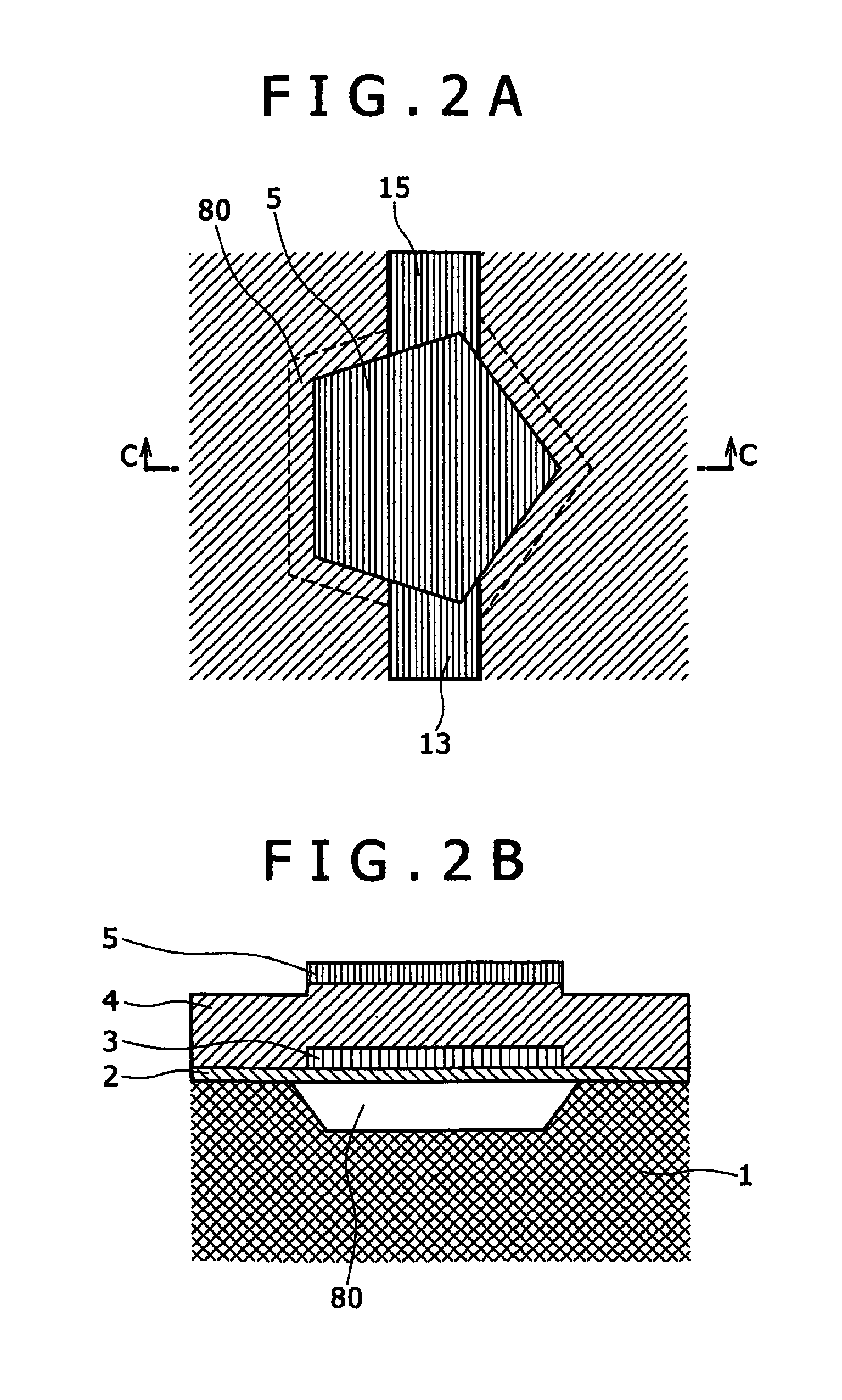
[0047]FIG. 5A is a top schematic view of a film bulk acoustic wave resonator according to a second embodiment, and FIG. 5B is a cross-sectional schematic view of the film bulk acoustic wave resonator according to the first embodiment, which is taken along line D-D in FIG. 5A. Referring to FIGS. 5A and 5B, one example of the film bulk acoustic wave resonator according to the second embodiment of the present invention will be described. In the second embodiment, the film bulk acoustic wave resonator includes a laminate-structured resonance part 20 which is formed on an insulating substrate 1 and composed of a piezoelectric layer 4, a first electrode layer 3 serving as a lower electrode, and a second electrode layer 5 serving as an upper electrode, the first and second electrode layers interposing at least part of the piezoelectric layer 4 between them. The first metal electrode 3 is dispersively formed on an electrode plane facing the second metal electrode 5, and a gap 80 is formed i...
embodiment 3
[0056]FIG. 8A is a top schematic view of a film bulk acoustic wave resonator according to a third embodiment, and FIG. 8B is a cross-sectional schematic view of the film bulk acoustic wave resonator according to the third embodiment, which is taken along line G-G in FIG. 8A. Referring to FIGS. 8A and 8B, one example of the film bulk acoustic wave resonator according to the third embodiment of the present invention will be described. In the third embodiment, the film bulk acoustic wave resonator includes a laminate-structured resonance part 20 which is formed on an insulating substrate 1 and composed of a piezoelectric layer 4, a first electrode layer 3 serving as a lower electrode, and a second electrode layer 5 serving as an upper electrode, the first and second electrode layers interposing at least part of the piezoelectric layer 4 between them. The first metal electrode 3 is dispersively formed on an electrode plane facing the second metal electrode 5, and a gap 80 is formed in t...
PUM
| Property | Measurement | Unit |
|---|---|---|
| radio frequency | aaaaa | aaaaa |
| diameter | aaaaa | aaaaa |
| width | aaaaa | aaaaa |
Abstract
Description
Claims
Application Information
 - R&D
- Intellectual Property
- Life Sciences
- Materials
- Tech Scout
- Unparalleled Data Quality
- Higher Quality Content
- 60% Fewer Hallucinations
Browse by: Latest US Patents, China's latest patents, Technical Efficacy Thesaurus, Application Domain, Technology Topic, Popular Technical Reports.
© 2025 PatSnap. All rights reserved.Legal|Privacy policy|Modern Slavery Act Transparency Statement|Sitemap|About US| Contact US: help@patsnap.com


