Low power pulse-triggered flip-flop

a low-power, pulse-triggered technology, applied in pulse generators, pulse techniques, electrical equipment, etc., can solve the problems of increased power loss, flip-flops used in high-order system circuits that do not maintain a constant triggered operation, and increase the total leakage power, so as to reduce circuit power consumption, shorten discharge routes, and increase processing speed

Inactive Publication Date: 2011-06-14
NATIONAL YUNLIN UNIVERSITY OF SCIENCE AND TECHNOLOGY
View PDF2 Cites 2 Cited by
  • Summary
  • Abstract
  • Description
  • Claims
  • Application Information

AI Technical Summary

Benefits of technology

By means of the structure set forth above, the low power pulse-triggered flip-flop of the present invention is formed. It provides many benefits, notably:
1. The present invention is a logic gate circuit adopted a Pass Transistor Logic (PTL) architecture to shorten discharge route. It is incorporated with a Conditional Pulse Enhancement Technique to further reduce circuit power consumption. Through these two novel circuits the transistor dimension (and capacitor load) of the Delay Inverter and pulse generation circuit on the clock system can be shrunk. Compared with the conventional design increasing processing speed constantly, the present invention provides a circuit of lower power consumption to extend product working time and prevent elements from heat loss. The lower power circuit design can meet specification requirements and reduce power waste, and further lower power consumption when in use.
2. The present invention employs Post-Layout Simulation of UMC CMOS 90 nm fabrication process technique. The results show that power consumption and Power-Delay-Product save more than 17%. Coupled with the shrunk total transistor size, the design provided by the present invention reduces 2.4 times of average leakage current power loss.

Problems solved by technology

As the chip function becomes more diversified and complex, and clock frequency and total number of transistors decrease gradually, total leakage power becomes more severe.
Design of low power circuits, therefore, becomes very important to reduce power consumption of the chip becomes a big issue and research focus at present.
Because the SoC clock circuit and storage circuit are the main cause of power loss, design of a lower power storage element becomes a critical factor to reduce total power consumption of SoC.
However, the flip-flop used on high order system circuits do not maintain a constant triggered operation, but always in a standby state.
Since the pulse clock of PTFF is maintained at the same width and intensity, extra power loss incurs.
While PTFF can improve some drawbacks of the conventional flip-flop as previously discussed, at present there are no design and research reports that have announced regard changing circuit pulse width and intensity according to input data of flip-flop.

Method used


Image

  • Low power pulse-triggered flip-flop
  • Low power pulse-triggered flip-flop
  • Low power pulse-triggered flip-flop

Examples


Embodiment Construction

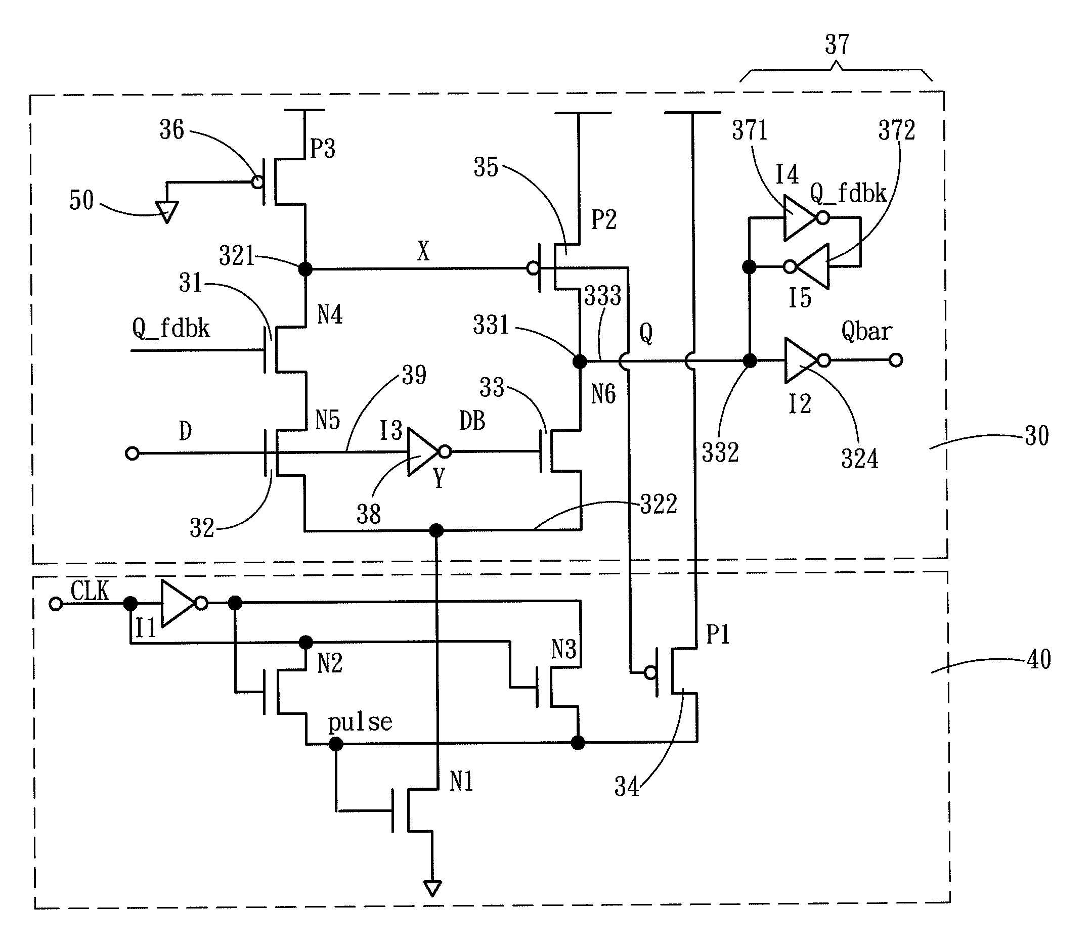
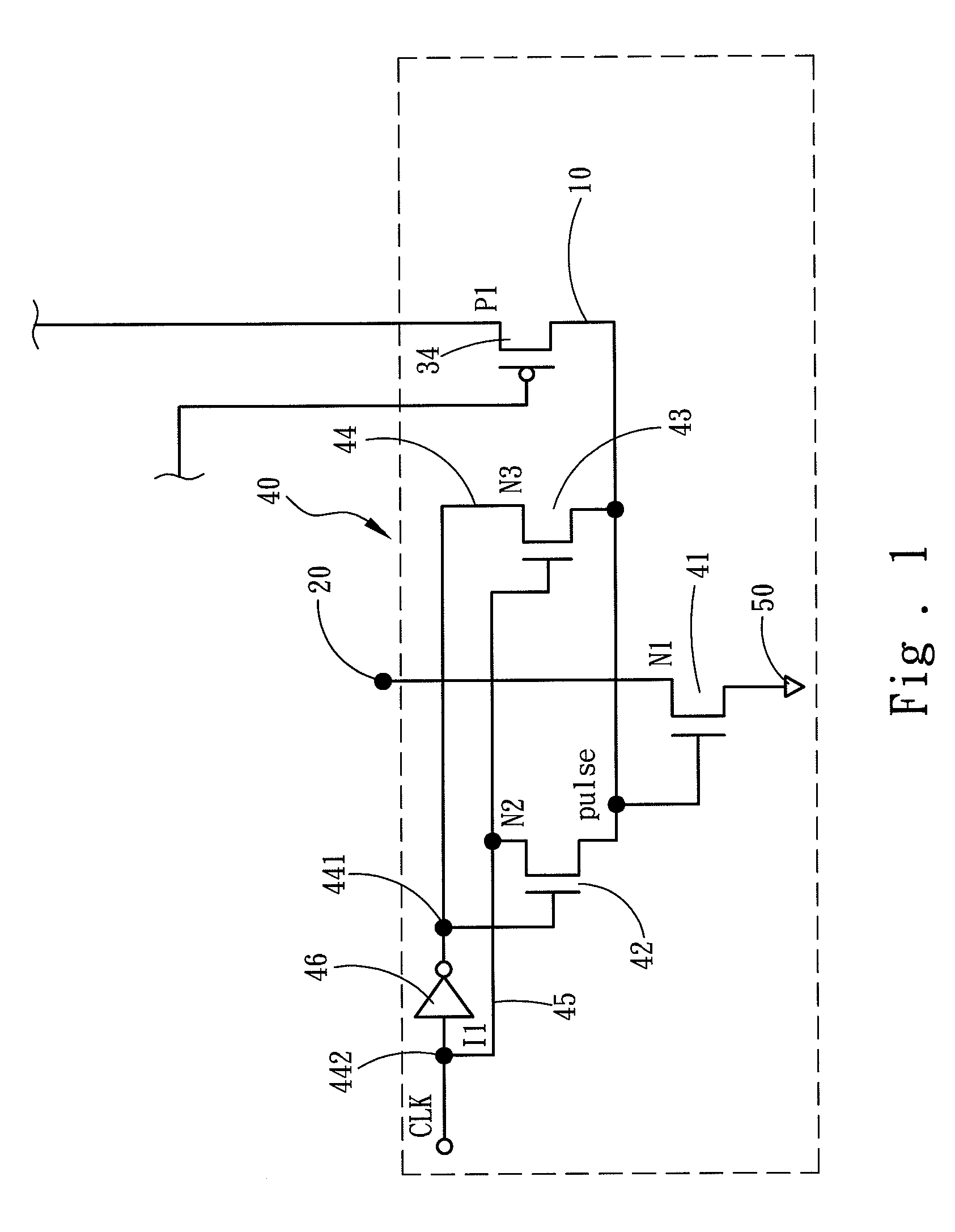
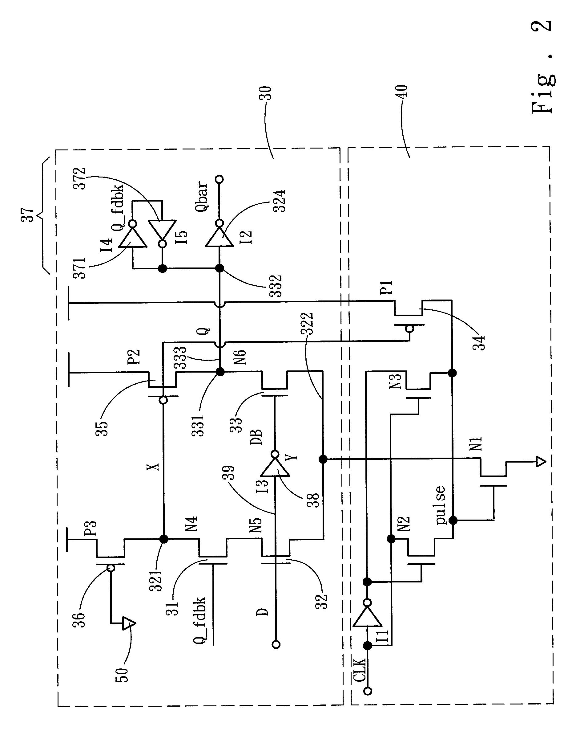
Refer to FIG. 1 and FIG. 2. The low power pulse-triggered flip-flop according to the present invention comprises a latch 30 containing a first conductive line 10 and a first connection point 20 and a pulse generator 40 linking to the latch 30. The pulse generator 40 includes a first N-transistor 41, a second N-transistor 42, a third N-transistor 43, a first P-transistor 34 and a first inverter 46. The first N-transistor 41 has a gate, a first end and a second end. The first end of the first N-transistor 41 is connected to the first connection point 20. The gate of the first N-transistor 41 is connected to the first conductive line 10. The second end of the first N-transistor 41 is connected to a ground 50.

The second N-transistor 42 has a gate, a first end and a second end. The second end of the second N-transistor 42 is connected to the first conductive line 10.

The third N-transistor 43 has a gate, a first end and a second end. The second end of the third N-transistor 43 is connecte...


PUM


Abstract

A low power pulse-triggered flip-flop comprises a latch containing a first conductive line and a first connection point and a pulse generator linking to the latch. The pulse generator includes a first N-transistor, a second N-transistor, a third N-transistor, a first inverter and a first P-transistor located on the first conductive line. The first N-transistor is connected to the first connection point and first conductive line. The second N-transistor and the third N-transistor are connected to the first conductive line, a second conductive line and a third conductive line. The first inverter is connected to the second conductive line. The present invention aims to reduce leakage power in a high level fabrication process, and can save power consumption and power-delay-product more than 17% over the conventional pulse triggered flip-flop, and also provides a smaller size of total transistors to lower average leakage current power consumption by 2.4 times.

Description

FIELD OF THE INVENTIONThe present invention relates to a circuit design of flip-flop and particularly to a low power pulse-triggered flip-flop.BACKGROUND OF THE INVENTIONConventional very large scale integrated circuit (VLSI) systems rely on System on a Chip (SoC) to achieve higher performance and receive more diversified architectures. As the chip function becomes more diversified and complex, and clock frequency and total number of transistors decrease gradually, total leakage power becomes more severe. Design of low power circuits, therefore, becomes very important to reduce power consumption of the chip becomes a big issue and research focus at present.Because the SoC clock circuit and storage circuit are the main cause of power loss, design of a lower power storage element becomes a critical factor to reduce total power consumption of SoC.Flip-Flop (FF) is an important and widely used storage element, especially on mobile devises such as notebook computers, personal digital ass...

Claims


Application Information

Patent Timeline
IPC IPC(8): H03K3/356
CPCH03K3/356173H03K3/012
Inventor LIN, JIN-FACHO, YU-RUSHEU, MING-HWA
Owner NATIONAL YUNLIN UNIVERSITY OF SCIENCE AND TECHNOLOGY
Why Eureka
Try Eureka