Photodiode array having semiconductor substrate and crystal fused regions and method for making thereof

a photodiode array and crystal fused region technology, applied in the field of photodiode arrays, can solve the problems of cross talk between photodiodes and photodiodes, and achieve the effects of preventing cross talk, simple step, and maintaining mechanical strength

Active Publication Date: 2011-06-14
HAMAMATSU PHOTONICS KK
View PDF14 Cites 0 Cited by
  • Summary
  • Abstract
  • Description
  • Claims
  • Application Information

AI Technical Summary

Benefits of technology

[0008]The present invention provides a photodiode array capable of being formed by a simple step and of preventing cross talk while maintaining the mechanical strength, and a method for making the same.
[0010]The above-mentioned photodiode array is provided with crystal fused regions formed between the plurality of photodiodes. The semiconductor material loses the crystallinity in the crystal fused regions. Since the crystal fused region prevents carriers from leaking to the adjoining photodiode, cross talk between the plurality of photodiodes can be suitably prevented.
[0011]Means for preventing cross talk can be obtained by only forming the crystal fused region in the above-mentioned photodiode array. Therefore, the above-mentioned photodiode array can simplify the manufacturing process as compared with the conventional photodiode array requiring the step of forming the trench groove and the insulating layer, and the step of filling the trench groove. Since the above-mentioned photodiode array is not provided with a physical groove, the mechanical strength of the photodiode array can be maintained.
[0014]In the above-mentioned photodiode array, the crystal fused regions are formed so as to reach the semiconductor substrate from the surface of the first semiconductor layer. Thereby, cross talk between the photodiodes constituted by the first semiconductor layer and the second semiconductor layer can be more effectively prevented.
[0016]In the above-mentioned method for making the photodiode array, the photodiode is constituted by the pn junction of the first semiconductor layer and second semiconductor layer. The first semiconductor layer and the semiconductor substrate are fused to lose the crystallinity in the crystal fused region. Therefore, since the crystal fused regions for preventing the carriers from leaking to the adjoining photodiode can be suitably formed by the above-mentioned method for making the photodiode array, the photodiode array can be provided, which can suitably prevent cross talk between the plurality of photodiodes.

Problems solved by technology

The greatest problem of the multichannel photodiode and photodiode array is cross talk between pixels.

Method used


Image

  • Photodiode array having semiconductor substrate and crystal fused regions and method for making thereof
  • Photodiode array having semiconductor substrate and crystal fused regions and method for making thereof
  • Photodiode array having semiconductor substrate and crystal fused regions and method for making thereof

Examples


Embodiment Construction

[0032]Hereafter, a photodiode array according to an embodiment of the present invention will be explained. Identical components are designated by the same reference numerals, and overlapping description is omitted.

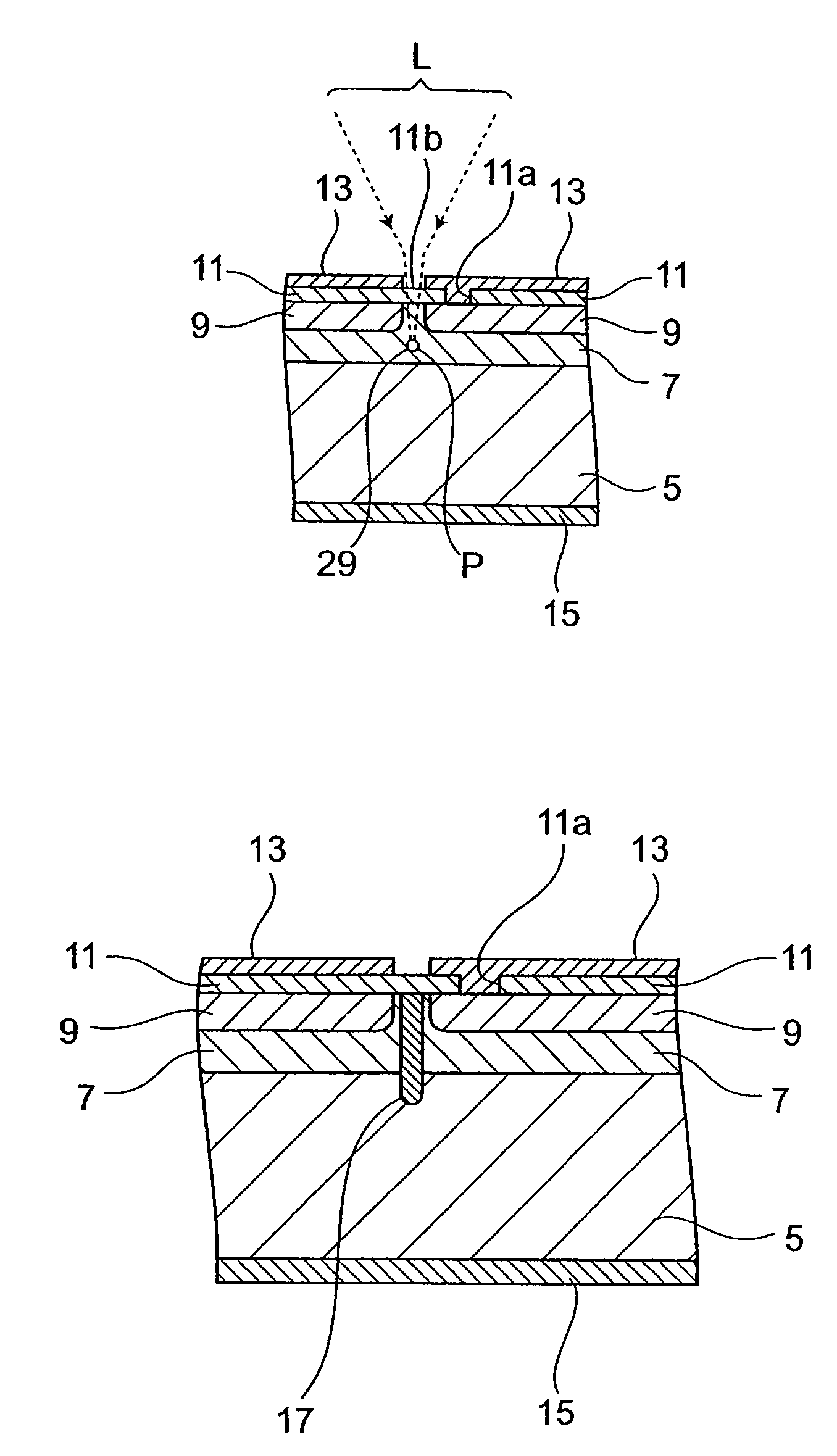
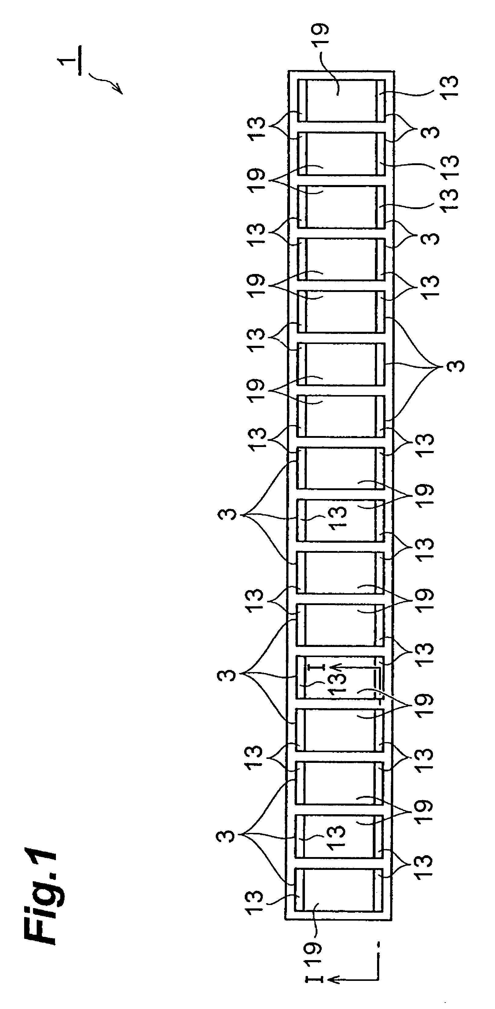
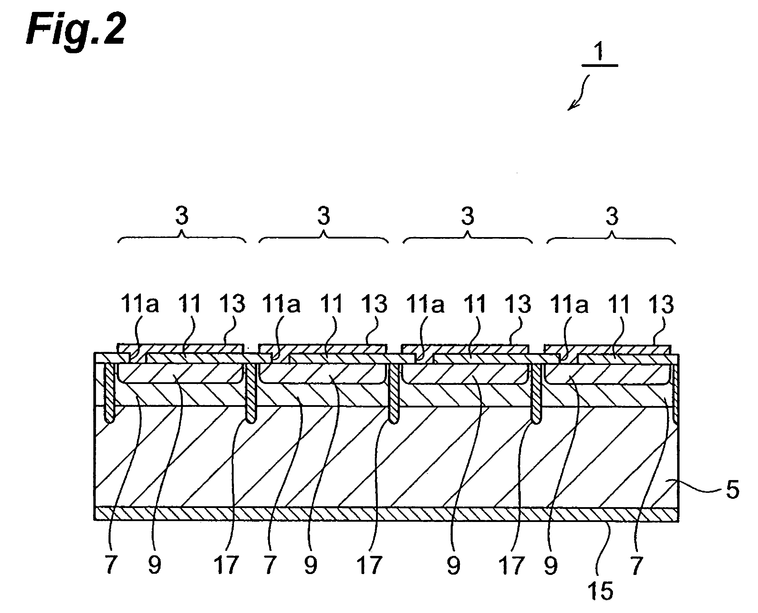
[0033]FIG. 1 is a plan view showing an embodiment of a photodiode array according to the present invention. FIG. 2 is a sectional view showing the I-I section of the photodiode array shown in FIG. 1. In the photodiode array 1 according to the embodiment, a plurality of photodiodes 3, for embodiment, of 16 pieces are one-dimensionally arranged.

[0034]With reference to FIG. 1, each of the photodiodes 3 has a photodetecting region 19. The photodiode 3 has a surface electrode 13 formed at the both ends of the photodetecting region 19.

[0035]With reference to FIG. 2, the photodiode array 1 is provided with a semiconductor substrate 5 consisting of an n-type semiconductor, a first semiconductor layer 7 formed on the semiconductor substrate 5 and consisting of a semiconductor havin...


PUM


Abstract

Disclosed is a photodiode array comprising a semiconductor substrate; a plurality of photodiodes formed on the semiconductor substrate; and crystal fused regions losing crystallinity by fusing a semiconductor material of the photodiodes between the plurality of photodiodes.

Description

[0001]This is a divisional application of application Ser. No. 11 / 333,544, filed on Jan. 18, 2006, now abandoned which is incorporated by reference herein in its entirety.BACKGROUND OF THE INVENTION[0002]1. Field of the Invention[0003]The present invention relates to a photodiode array.[0004]2. Related Background of the Invention[0005]A multichannel photodiode and a photodiode array have been known as a photodetecting element having a plurality of pixel regions formed on the same substrate. The greatest problem of the multichannel photodiode and photodiode array is cross talk between pixels.[0006]As a method for preventing cross talk between the pixels, for embodiment, a structure where trench grooves are formed between the pixels and the trench grooves are filled with an insulating material to maintain the mechanical strength is disclosed in Japanese Patent Laid-Open Publication No. 2001-352094. FIG. 13 is a sectional view showing a photodiode array disclosed in Japanese Patent Lai...

Claims


Application Information

Patent Timeline
Patent Type & Authority Patents(United States)
IPC IPC(8): H01L21/00
CPCH01L27/1443H01L27/14683H01L27/1463H01L27/1446
Inventor FUJII, YOSHIMAROOKAMOTO, KOUJISAKAMOTO, AKIRA
Owner HAMAMATSU PHOTONICS KK
Why Eureka
Try Eureka