
Scanning probe devices and methods for fabricating same

a scanning probe and probe body technology, applied in the direction of mechanical measurement arrangement, mechanical roughness/irregularity measurement, instruments, etc., can solve the problems of inherently large radius of curvature of the tip, poor sharpness of the tip, and difficulty in controlling the thickness of the fabricated cantilever of less than about 1 m of silicon, etc., to achieve the effect of easy fabrication

Active Publication Date: 2011-03-29
APPLIED NANOSTRUCTURES
View PDF14 Cites 25 Cited by
  • Summary
  • Abstract
  • Description
  • Claims
  • Application Information

AI Technical Summary

Benefits of technology

[0019]Briefly, and in general terms, the present invention is directed to scanning probe structures that overcome these and other deficiencies, and methods for fabricating the probes. The advantages provided by such probes and methods can include probe designs in which a soft, reflective coating is optional and the tips may be extremely sharp, easy to fabricate, and display flexibility with respect to chemical modification, particularly functionalization.

Problems solved by technology

Since the cantilever thickness in silicon probes is usually controlled by an etching process, it is very difficult to control a fabricated cantilever thickness of less than about 1 μm of silicon with high percentage of yield and uniformity across the wafer.
The tip is molded out of an inverted pyramidal shape pit made in the silicon wafer; as a result, the tips suffer from poor sharpness.
The radius of curvature of these tips is inherently large due to process limitations.
These methods have limitation of controlling exposure of the tip to uncover the apex.
The silicon nitride surface is typically hydrophilic in nature and therefore has limited application with respect to tip functionalization.
In addition, the exposed surface area of the tip in probes having cantilevers with integrated silicon tips is generally too small for functionalization.
The degree of bending is of the same order of the magnitude as of features in many samples useful for nanotechnology applications, thereby limiting the resolution of the probe.
For example, resolving some minute biological entities such as virus particles in liquid, particularly those having sub-nanometer features, is difficult with metal coated cantilevers.
(1) an optional layer of metal must be deposited on the probe to facilitate or improve reflection;
(2) tips fabricated from silicon nitride are not sharp enough for many applications;
(3) tips fabricated from silicon nitride are limited with respect to tip functionalization; and
(4) integrated silicon tips are difficult to fabricate, particularly with respect to controlling exposure of the apex.

Method used


Image

  • Scanning probe devices and methods for fabricating same
  • Scanning probe devices and methods for fabricating same
  • Scanning probe devices and methods for fabricating same

Examples


Embodiment Construction

[0037]The following description presents preferred embodiments of the invention representing the best mode contemplated for practicing the invention. This description is not to be taken in a limiting sense but is made merely for the purpose of describing the general principles of the invention whose scope is defined by the appended claims.

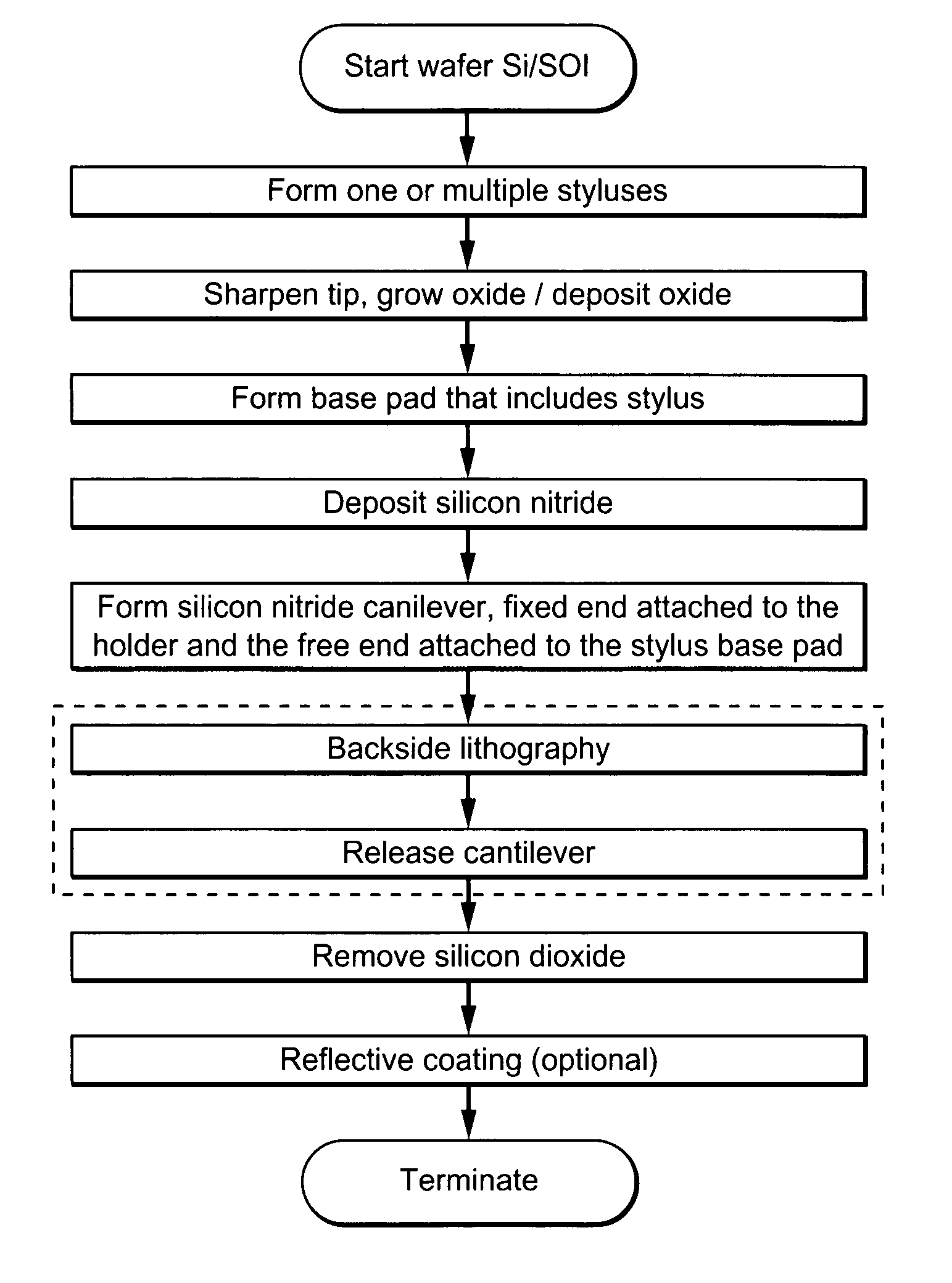
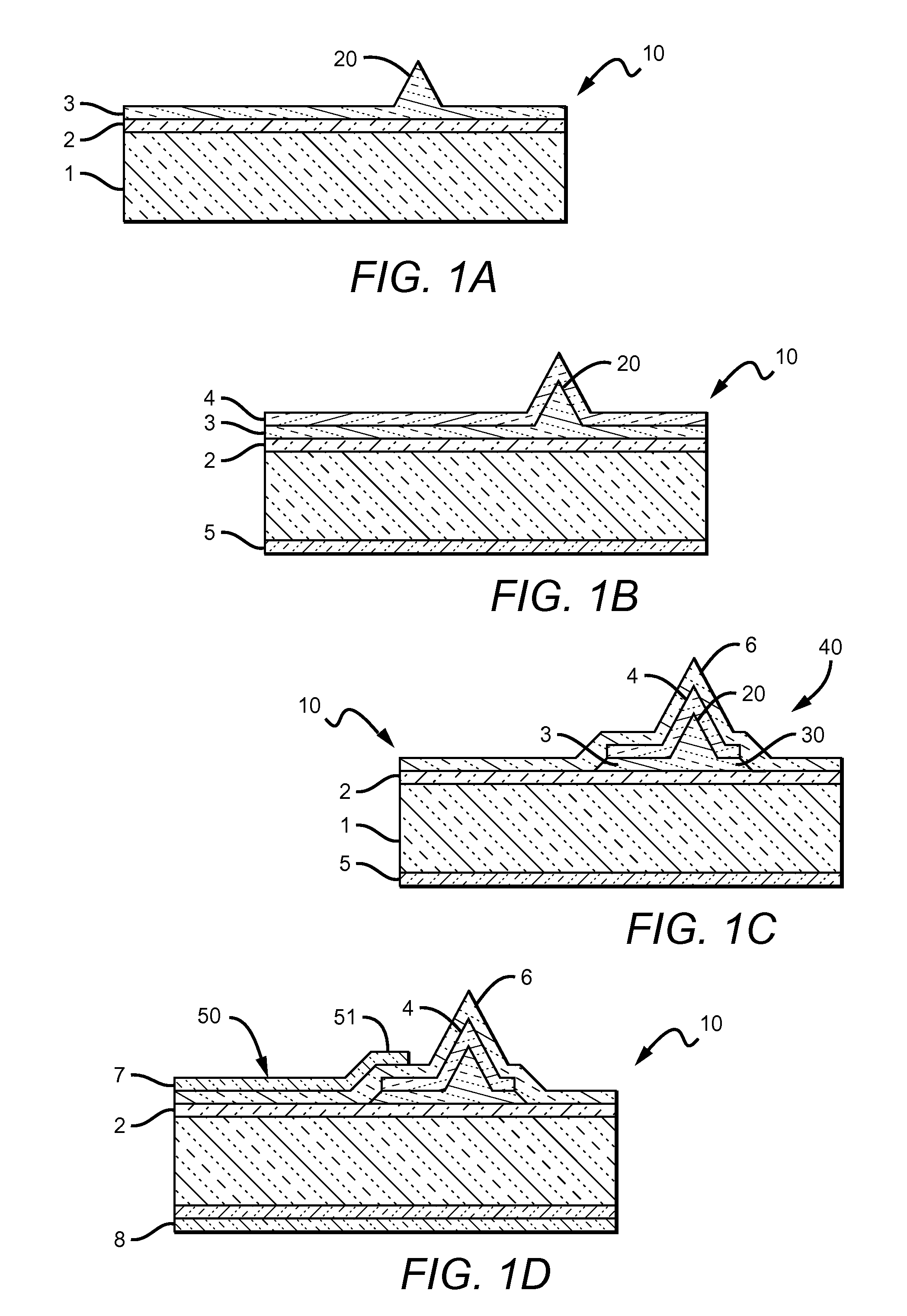
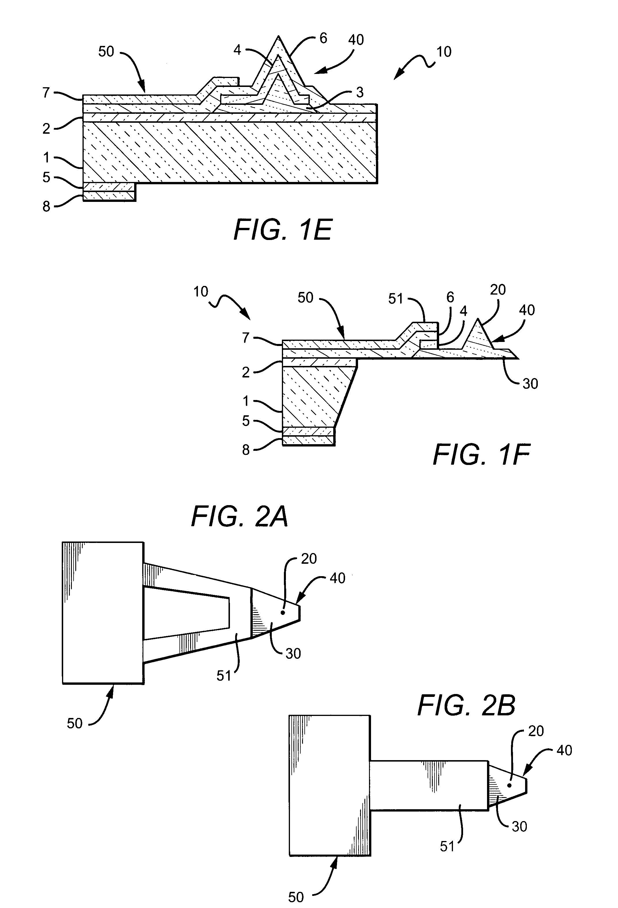
[0038]The present invention provides scanning probes in which a cantilever contacts a stylus via an integrated stylus base pad, and methods for fabricating such probes. The probe offers many advantages over other types of scanning probes with respect to tip sharpness, optional reflective coating, flexibility with respect to functionalizing the tip, and minimal thermal drift due to reduced bimorph effect. These features facilitate the acquisition of high resolution images of samples in general, and particularly in liquids.

[0039]Other features and advantages of the invention will be apparent from the following detailed description when taken together...


PUM

PropertyMeasurementUnit
Widthaaaaaaaaaa
Reflectionaaaaaaaaaa

Abstract

The present invention is directed to scanning probes in which a cantilever contacts a stylus via an integrated stylus base pad, and methods for fabricating such probes. The probe offer many advantages over other types of scanning probes with respect to eliminating the need for a soft, reflective coating in some applications and providing for the simple fabrication of sharp stylus tips, flexibility with respect to functionalizing the tip, and minimal thermal drift due to reduced bimorph effect. The advantage of these features facilitates the acquisition of high resolution images of samples in general, and particularly in liquids.

Description

CROSS REFERENCE TO RELATED APPLICATION[0001]This application claims priority to the earlier provisional application entitled “Method of making scanning probes and process of batch manufacturing thereof,” Ser. No. 60 / 859,344, filed Nov. 15, 2006, the disclosures of which are hereby incorporated herein by reference.BACKGROUND[0002]1. Field of the Invention[0003]The present invention relates generally to surface probing devices and methods for making the devices and, more particularly, to the design and fabrication of scanning probes.[0004]2. Description of the Related Art[0005]Scanning Probe Microscopy (SPM) is a general term used to describe a growing number of techniques that use a sharp probe to scan over a surface and measure some property of that surface. The major advantage of scanning probe microscopy is that the resolution of the microscopes is not limited by diffraction, as is the case when using a beam of light or electrons, but only by the size of the probe-sample interacti...

Claims


Application Information

Patent Timeline
IPC IPC(8): G01Q70/16
CPCB82Y35/00G01Q70/16G01Q70/10
Inventor CHAND, AMI
Owner APPLIED NANOSTRUCTURES
Learn More