Diketopyrrolopyrrole-based derivatives for thin film transistors
a technology of diketopyrrolopyrrole and derivatives, which is applied in the direction of diketopyrrolopyrrole dyes, thermoelectric devices, solid-state devices, etc., can solve the problems of preventing the fabrication of tfts in ambient conditions, and not being suitable for ambient fabrication of devices
- Summary
- Abstract
- Description
- Claims
- Application Information
AI Technical Summary
Benefits of technology
Problems solved by technology
Method used
Image
Examples
example 1
Synthesis of Poly(2,5-dioctadecyl-3,6-bis(thienyl-5-yl)-diketopyrrolopyrrole
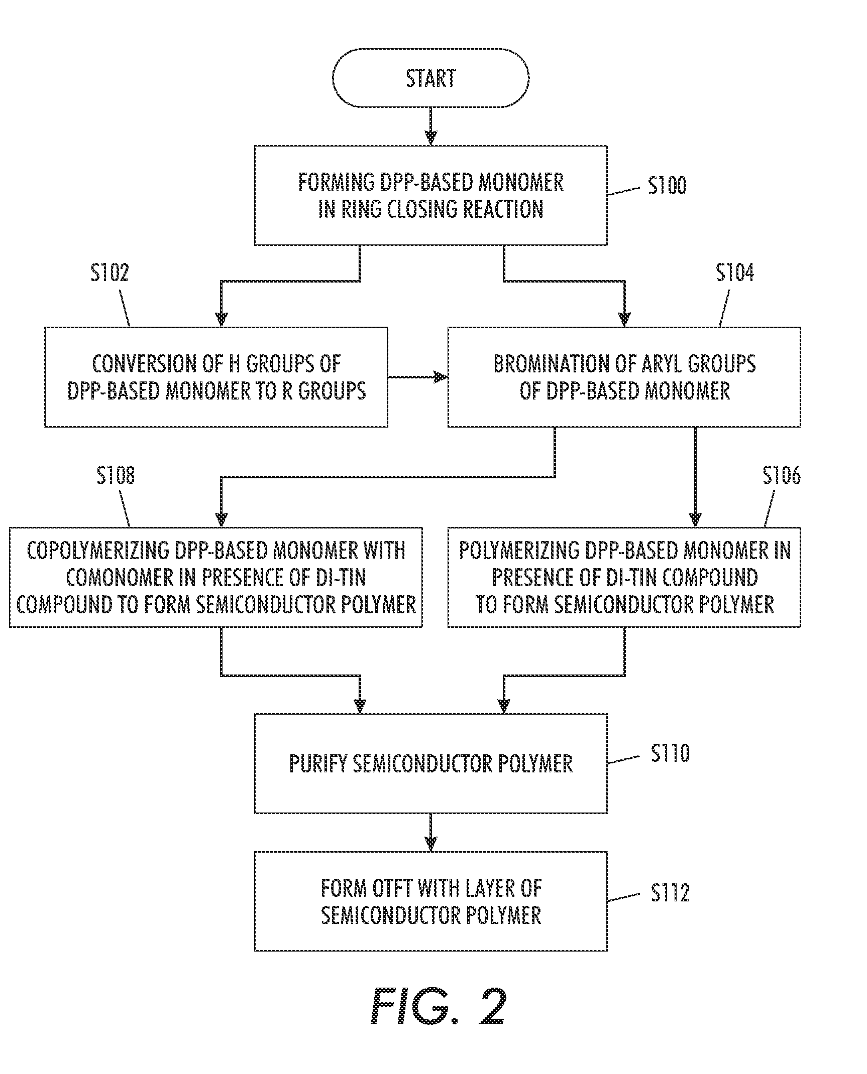
[0124]The synthesis of a representative polymer 4 is outlined in Scheme 1
[0125]
[0126]The experimental details are described as follows.
1. Synthesis of 3,6-Bis-(thienyl)-diketopyrrolopyrrole (1)
[0127]Sodium (3.45 g, 0.15 mol) was added to 60 mL of t-amyl alcohol and a small amount of iron(III) chloride (50 mg) was added. The mixture was stirred vigorously for 1 hr at 95-102° C. until sodium disappeared. The solution was cooled to 85° C. To the resultant solution was added 10.9 g (0.1 mol) of 2-thiophenecarbonitrile. Then, 8.3 g (0.04 mol) of diisopropyl succinate in 5 mL of t-amyl alcohol was added drop-wise over 1 h at 85° C. When addition was complete, the mixture was maintained for 2 hr at this temperature. The reaction mixture was then cooled to 50° C., diluted with 50 mL of methanol, and then slowly neutralized with ˜15 mL of glacial acetic acid and refluxed briefly, and the reaction mixture was filtered...
example 2
OTFT Fabrication and Characterization
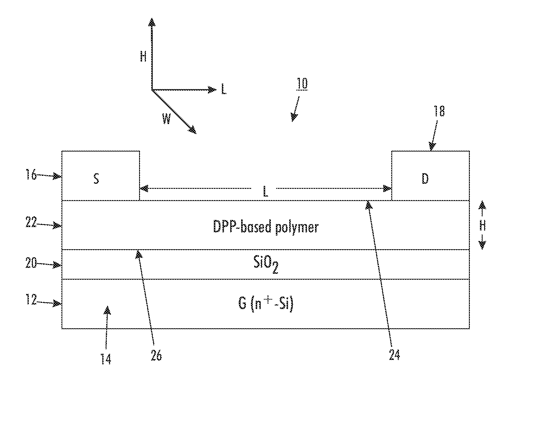
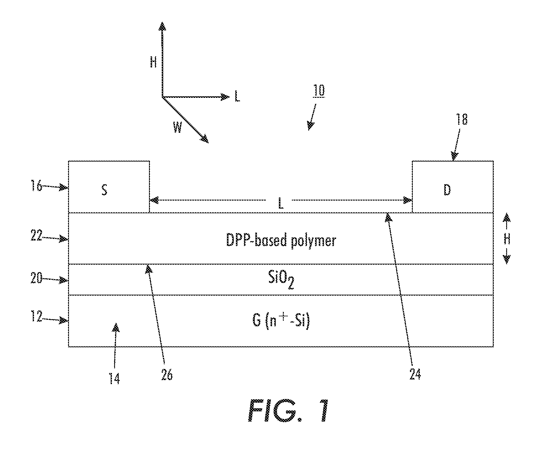
[0131]A top-contact thin film transistor configuration as schematically illustrated in FIG. 1 was selected as a test device structure. The test device was built on an n-doped silicon wafer with a thermally grown silicon oxide layer 20 with a thickness of about 200 nanometers thereon, and had a capacitance of about 15 nF / cm2 (nanofarads / square centimeter), as measured with a capacitor meter. The wafer functioned as the gate electrode while the silicon oxide layer acted as the gate dielectric.
[0132]The n-doped silicon wafer with silicon oxide layer thereon was first cleaned with isopropanol, argon plasma, isopropanol and air dried, and then immersed in a 0.1 M solution of octyltrichlorosilane (OTS-8) in toluene at 60° C. for 20 min. Subsequently, the wafer was washed with toluene, isopropanol and air-dried. A solution of polymer (4) (poly(2,5-dioctadecyl-3,6-bis(thienyl-5-yl)-diketopyrrolopyrrole)) dissolved in dichlorobenzene (0.5 percent by weigh...
PUM
| Property | Measurement | Unit |
|---|---|---|
| thickness | aaaaa | aaaaa |
| thickness | aaaaa | aaaaa |
| thickness | aaaaa | aaaaa |
Abstract
Description
Claims
Application Information
 - R&D
- Intellectual Property
- Life Sciences
- Materials
- Tech Scout
- Unparalleled Data Quality
- Higher Quality Content
- 60% Fewer Hallucinations
Browse by: Latest US Patents, China's latest patents, Technical Efficacy Thesaurus, Application Domain, Technology Topic, Popular Technical Reports.
© 2025 PatSnap. All rights reserved.Legal|Privacy policy|Modern Slavery Act Transparency Statement|Sitemap|About US| Contact US: help@patsnap.com


