
Organic light-emitting diode display device and driving method thereof

a light-emitting diode display and organic technology, applied in static indicating devices, instruments, electroluminescent light sources, etc., can solve the problems of difficult manufacture as a wide-screen display screen, low light-emission efficiency and large power consumption, and the charging characteristics of data lines deteriorate, so as to reduce the charging time of data lines, prevent residual image problems, and improve picture quality uniformity

Active Publication Date: 2011-02-15
LG DISPLAY CO LTD
View PDF5 Cites 14 Cited by
  • Summary
  • Abstract
  • Description
  • Claims
  • Application Information

AI Technical Summary

Benefits of technology

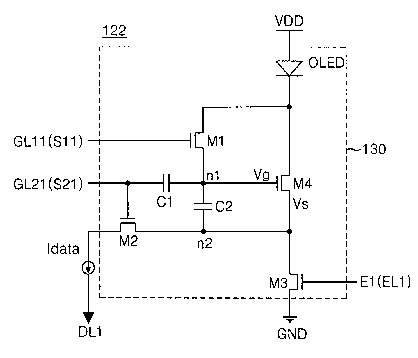
The invention is about an organic light-emitting diode display device and a driving method thereof that solves problems of previous devices. The technical effects of the invention include reducing data line charging time, improving picture quality uniformity, preventing residual image problem, and increasing data charging time upon driving a low-level gray scale while reducing bias stress burden on the driving TFT upon driving a high-level gray scale. The invention includes a data line, first and second gate lines, an emission line, an organic light-emitting diode device, a first switch element, a second switch element, a third switch element, a driving element, a first capacitor, and a second capacitor. The driving method involves supplying a high-level potential driving voltage to the anode electrode, connecting the cathode electrode to a first node through a first switch element, connecting the data line to a second node through a second switch element, connecting the second node to a ground voltage source through a third switch element, adjusting a current flowing between the cathode electrode and the first node through the driving element in response to a voltage on the first node, and emitting light from the organic light-emitting diode device.

Problems solved by technology

However, each of these flat panel devices has advantages and drawbacks.
The PDP has light weight, thin profile and wide screen display capability because its structure and manufacturing process are simple, but yet it has low light-emission efficiency and large power consumption.
An active matrix LCD employing a thin film transistor (hereinafter, referred to as “TFT”) as a switching device has the drawback in that it is difficult to manufacture as a wide screen display screen because a semiconductor manufacturing processes are used, but the active matrix display is in high demand since it is typically used for a display device of a notebook personal computer.
A charging characteristics on the data line deteriorates due to the effect of a parasitic capacitance with the data line while driving at a low-level.
When the related art organic light-emitting diode display device driven in accordance with a current drive method is driven at a low current level, then the problem of increased charging time occurs.
But a proportional relationship between T2 and T1 is not always constantly maintained, and a difference between the pixels is generated by non-uniformities among the TFTs or a TFT deterioration.
Accordingly, the related art organic light-emitting diode display device has a drawback of picture quality detioration.
Because the related art organic light-emitting diode display device up-scales a current level in a constant ratio irregardless of a gray scale, there is also a problem in that a current for charging a data line is not enough in the case of a lower gray scale to be up-scaled in a relatively high ratio, and a bias stress of the driving TFT is increased for the case of a higher gray scale to be up-scaled in a relatively low ratio.

Method used


Image

  • Organic light-emitting diode display device and driving method thereof
  • Organic light-emitting diode display device and driving method thereof
  • Organic light-emitting diode display device and driving method thereof

Examples


Embodiment Construction

[0039]Reference will now be made in detail to the preferred embodiments of the invention, examples of which are illustrated in the accompanying drawings. The invention may, however, be embodied in many different forms and should not be construed as being limited to the embodiments set forth herein; rather, these embodiments are provided so that this disclosure will be thorough and complete, and will fully convey the concept of the invention to those skilled in the art. Like reference numerals in the drawings denote like elements.

[0040]FIG. 4 is a block diagram showing an organic light-emitting diode display device according to an embodiment of the invention, and FIG. 5 is a diagram showing signal pulses applied to k (k is a positive integer having a value of more than 1 and less than n)th pixels in a vertical direction of FIG. 4 and a data current. Referring to FIG. 4 and FIG. 5, an organic light-emitting diode display device according to an embodiment of the invention includes a di...


PUM


Abstract

An organic light-emitting diode display device includes a data line, a first and second gate lines crossing the data line, an emission line crossing the data line, an organic light-emitting diode device having an anode electrode and a cathode electrode, a high-level potential driving voltage source for supplying a high-level potential driving voltage to the anode electrode, a first switch element for connecting a cathode electrode of the organic light-emitting diode device to a first node, a second switch element for connecting the data line to a second node, a third switch element for connecting the second node to a ground voltage source, a driving element for adjusting a current flowing between the cathode electrode of the organic light-emitting diode device and the first node in accordance with a voltage of the first node, a first capacitor connected between the second gate line and the first node, and a second capacitor connected between the first node and the second node.

Description

[0001]This application claims the benefit of Korean Patent Application No. P06-0060543 filed in Korea on Jun. 30, 2006, which is hereby incorporated by reference in its entirety.BACKGROUND OF THE INVENTION[0002]1. Field of the Invention[0003]Embodiments of the present invention relates to a display device, and more particularly to an organic light-emitting diode display device and a driving method thereof. Although embodiments of the invention are suitable for a wide scope of applications, they are particularly suitable for reducing a data line charging time and preventing a residual image problem to improve a display quality.[0004]2. Description of the Related Art[0005]Recently, various flat panel display devices have been developed to have less weight and a thinner profile as compared to a cathode ray tube. Such flat panel display devices include a liquid crystal display device (hereinafter, referred to as “LCD”), a field emission display device (hereinafter, referred to as “FED”)...

Claims


Application Information

Patent Timeline
Patent Type & Authority Patents(United States)
IPC IPC(8): G09G3/32H05B44/00
CPCG09G3/3233G09G3/3283G09G2300/0819G09G2300/0852G09G2300/0861G09G2310/0248G09G2310/0251G09G3/30G09G3/32G09G3/20
Inventor YOO, JUHN SUK
Owner LG DISPLAY CO LTD
Learn More