Reducing inefficiencies of multi-clock-domain interfaces using a modified latch bank

a latch bank and multi-clock domain technology, applied in the field of electronic data transmission, can solve the problems of significant difficulties in resolving timing violations, embodiments may not contain any logical paths having an n:1 ratio, and embodiments may not contain any logical paths having an n:2 ratio, so as to achieve the effect of reducing space and performance inefficiencies of previous systems and allowing greater flexibility

Inactive Publication Date: 2011-02-01
IBM CORP
View PDF9 Cites 1 Cited by
  • Summary
  • Abstract
  • Description
  • Claims
  • Application Information

AI Technical Summary

Benefits of technology

[0038]The space and performance inefficiencies of previous systems may be partially eliminated by implementing a configuration that utilizes a modified latch bank with clock splitters and transmission gates in place of the latch bank and separate multiplexer of previous systems. Such a configuration may also yield greater flexibility for resolving timing criticalities at the data transmission interface.
[0039]The configuration disclosed reduces the number of devices necessary when compared to the implementation utilizing a latch bank and separate multiplexer. Further, as described in detail below, its structure allows for independent cycle stealing of the N:1 and N:2 logical paths, thus allowing for timing resolution solutions that use significantly fewer devices versus implementations that require the tuning of each individual bit in the cross-clock-domain interface. Therefore, the power and area savings of the disclosed embodiments may extend beyond those devices in the modified slave latch itself because timing criticalities that would otherwise have been resolved in the downstream logic may instead be resolved within the multi-domain interface itself.

Problems solved by technology

However, some embodiments may not contain any logical paths having an N:1 ratio.
However, some embodiments may not contain any logical paths having an N:2 ratio.
The multiplexer implementation of previous systems, such as the one of FIG. 1, causes significant difficulties with resolving timing violations.
In the case of logical paths that cross clock domains, the presence of skew and jitter may result in timing criticalities in any logical path, regardless of clock ratio.
Another limitation of the multiplexer implementation of FIG. 1 is that the multiplexer delay slows down the worst-case timing for the data path through the multiplexer 105.
Such adjustments commonly involve the usage of low voltage threshold (low-vt) devices or cycle stealing.
Such a solution also results in the logical path on the other side of a cycle-stolen latch having an allowable delay that is less than the clock period by the amount of the cycle-steal delay, which in some systems may cause another potential timing criticality and require further measures to stabilize the system.
Solving timing criticalities entirely with low-vt devices would require using a low-vt device in each multiplexer bypass path, which would result in a substantial increase in leakage power for most multi-bit interfaces.
However, as data transmissions have increased and circuits have become more complex, cycle stealing alone has often not been able to resolve all timing criticalities.
The tight timing characteristics of many modern systems have required both low-vt devices and cycle stealing to be implemented, often resulting in relatively low maximum worst case frequencies for logical paths.
Additionally, configurations that require a full bypass multiplexer for each bit of a cross-domain interface have large area and power requirements.

Method used


Image

  • Reducing inefficiencies of multi-clock-domain interfaces using a modified latch bank
  • Reducing inefficiencies of multi-clock-domain interfaces using a modified latch bank
  • Reducing inefficiencies of multi-clock-domain interfaces using a modified latch bank

Examples


Embodiment Construction

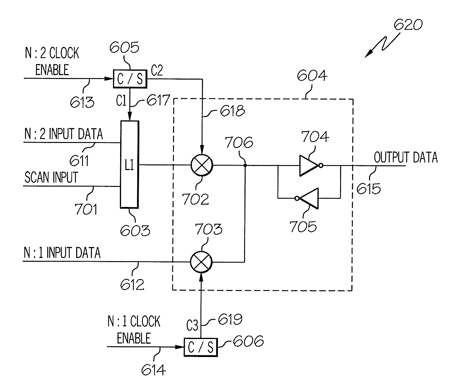
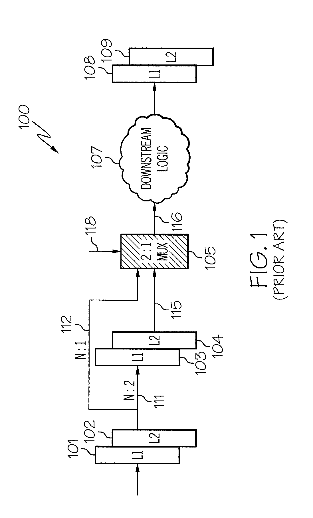
[0053]The present invention comprises a system and method for transmitting data between clock domains. In one embodiment of the present invention, the latch-and-multiplexer implementation of a cross-domain interface used in previous systems is integrated to save area and power and to improve mixed clock domain performance and efficiency. Further, some embodiments of the present invention allow for greater flexibility in resolving timing criticalities than do previous systems. The embodiments described in detail below contemplate synchronous clock domains. However, the system and method disclosed are applicable to any multi-clock-domain interface.

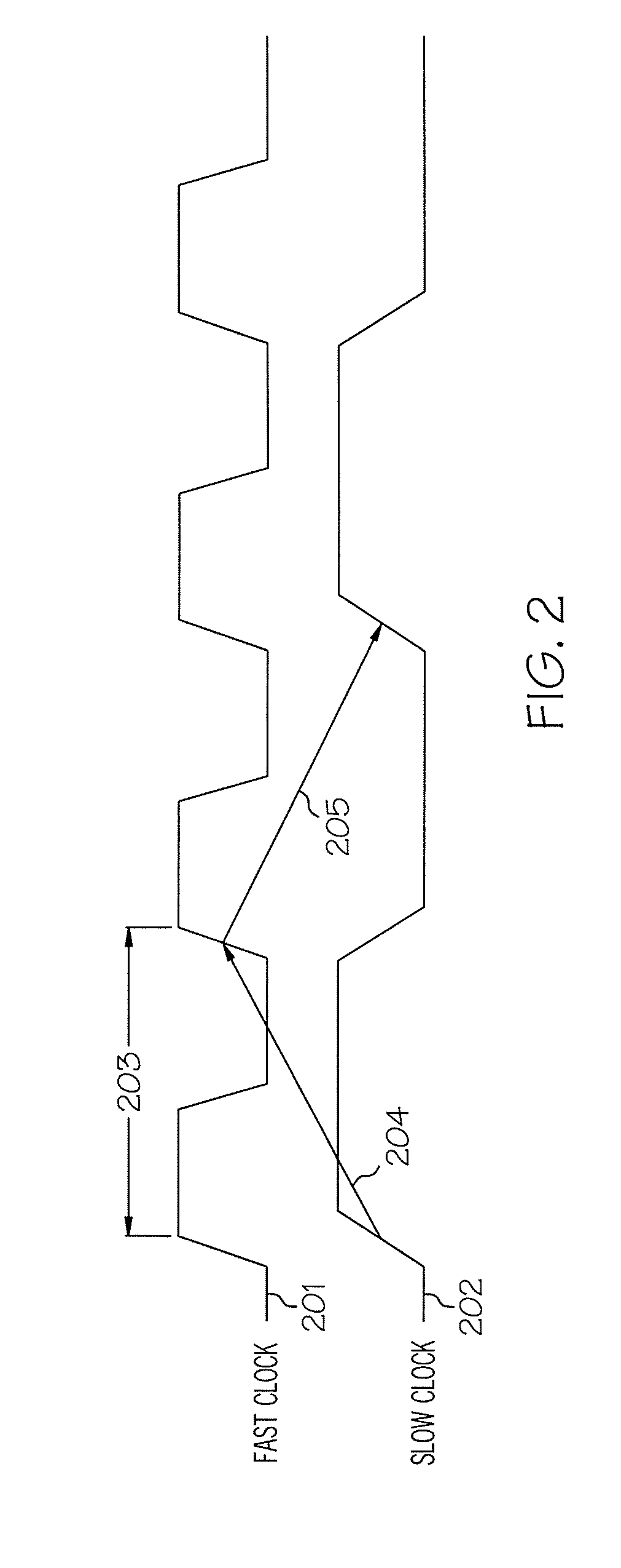
[0054]When a logical path crosses from one clock domain to another, the designer of a circuit or system takes into account the timing requirements for all valid clock ratios between the relevant clock domains. A domain may be any electronic domain that utilizes a digital clock. For example, in some embodiments, a domain may be a CPU interfac...


PUM


Abstract

A system and method for improving the performance and efficiency of multi-clock-domain data transmission interfaces. The data transmission interface may include a modified slave latch which includes one or more clock splitters and one or more transmission gates may be used. By having such a configuration, space requirements are reduced and a reduction of the number of devices necessary for a multi-domain interface may be realized. The configuration may further allow for independent cycle stealing of N:1 and N:2 logical paths, thus allowing for timing resolution solutions that use fewer devices versus implementations that require the tuning of each individual bit in the cross-clock-domain interface. By implementing such a data transmission interface, space and power requirements may be reduced and timing criticalities may be more easily managed.

Description

TECHNICAL FIELD[0001]The present invention relates to electronic data transmission, and more particularly to improving the performance and efficiency of multi-clock-domain data transmission interfaces by implementing an interface configuration including clock splitters and a modified latch bank.BACKGROUND INFORMATION[0002]Many electronic systems and applications require the transmission of data between clock domains of varying frequencies. When a logical path crosses from one clock domain to another, the designer of a circuit or system takes into account the timing requirements for all valid clock ratios between the relevant clock domains. The clock ratio between any two domains is typically defined as N:M, where N is the faster clock frequency and M is the slower clock frequency. The clock ratio between two clock domains determines the amount of delay allowed in a logical path that crosses between those clock domains.[0003]Logical implementations of cross-domain interfaces that sat...

Claims


Application Information

Patent Timeline
Patent Type & Authority Patents(United States)
IPC IPC(8): G06F1/04
CPCH04L7/02H04L7/0045
Inventor ARNOLD, NICOLE MARIEBAKER, MATTHEW WAYNEBOWERS, BENJAMIN JOHNCORREALE, JR., ANTHONYSTEINMETZ, PAUL MICHAEL
Owner IBM CORP
Why Eureka
Try Eureka