Semiconductor memory

a technology of semiconductors and memory, applied in the field of semiconductor memory, can solve the problems of data stored in the memory b>3/b> cannot be subjected to high-speed error correction, and take a long time to perform data error correction, so as to improve the speed of correction of data errors

Active Publication Date: 2011-01-25
PANASONIC SEMICON SOLUTIONS CO LTD
View PDF6 Cites 2 Cited by
  • Summary
  • Abstract
  • Description
  • Claims
  • Application Information

AI Technical Summary

Benefits of technology

[0013]The present invention is devised in order to solve the aforementioned conventional problems. An object of the present invention is to provide a semiconductor memory capable of correcting an error in data stored therein more promptly.
[0017]With this configuration, it is possible to perform arithmetic processing for error correction at a high-speed without an increase of connection terminals in number.
[0019]With this configuration, it is possible to facilitate timing control in synchronization with a clock, and to perform arithmetic processing for error correction with a clock timing unitized at maximum.
[0023]With this configuration, it is possible to perform arithmetic processing on data latched by the data latch in the semiconductor memory at a high speed. Thus, it is possible to perform data processing such as error correction more promptly.
[0025]Accordingly, the semiconductor memory can perform arithmetic processing on read data at a high speed to thereby invert such data. As a result, it is possible to write desired data to the semiconductor memory in a short period of time, and to perform data processing such as error correction more promptly.

Problems solved by technology

Consequently, it takes much time to perform error correction on data.
Therefore, there arises a problem that data stored in the memory 3 cannot be subjected to error correction at a high speed.

Method used


Image

  • Semiconductor memory
  • Semiconductor memory
  • Semiconductor memory

Examples


first embodiment

[0041]First, description will be given of a semiconductor memory according to a first embodiment of the present invention.

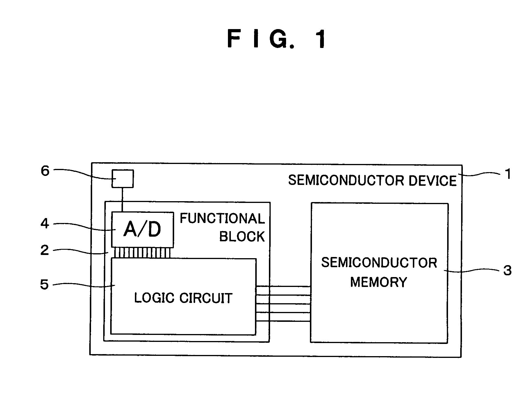
[0042]FIG. 1 is a block diagram showing a configuration of a semiconductor device on which the semiconductor memory according to the first embodiment is mounted. As shown in FIG. 1, the semiconductor device 1 includes a functional block 2, the semiconductor memory (hereinafter, simply referred to as “memory”) 3 according to the present invention, an analog-to-digital (hereinafter, abbreviated as “A / D”) converter 4, a logic circuit 5, and a pad 6.

[0043]Specifically, the semiconductor device 1 is configured by the functional block 2 and the memory 3. The functional block 2 is configured by the logic circuit 5 and the A / D converter 4. The logic circuit 5 is electrically connected to the A / D converter 4 and the memory 3. The pad 6 is connected to the A / D converter 4.

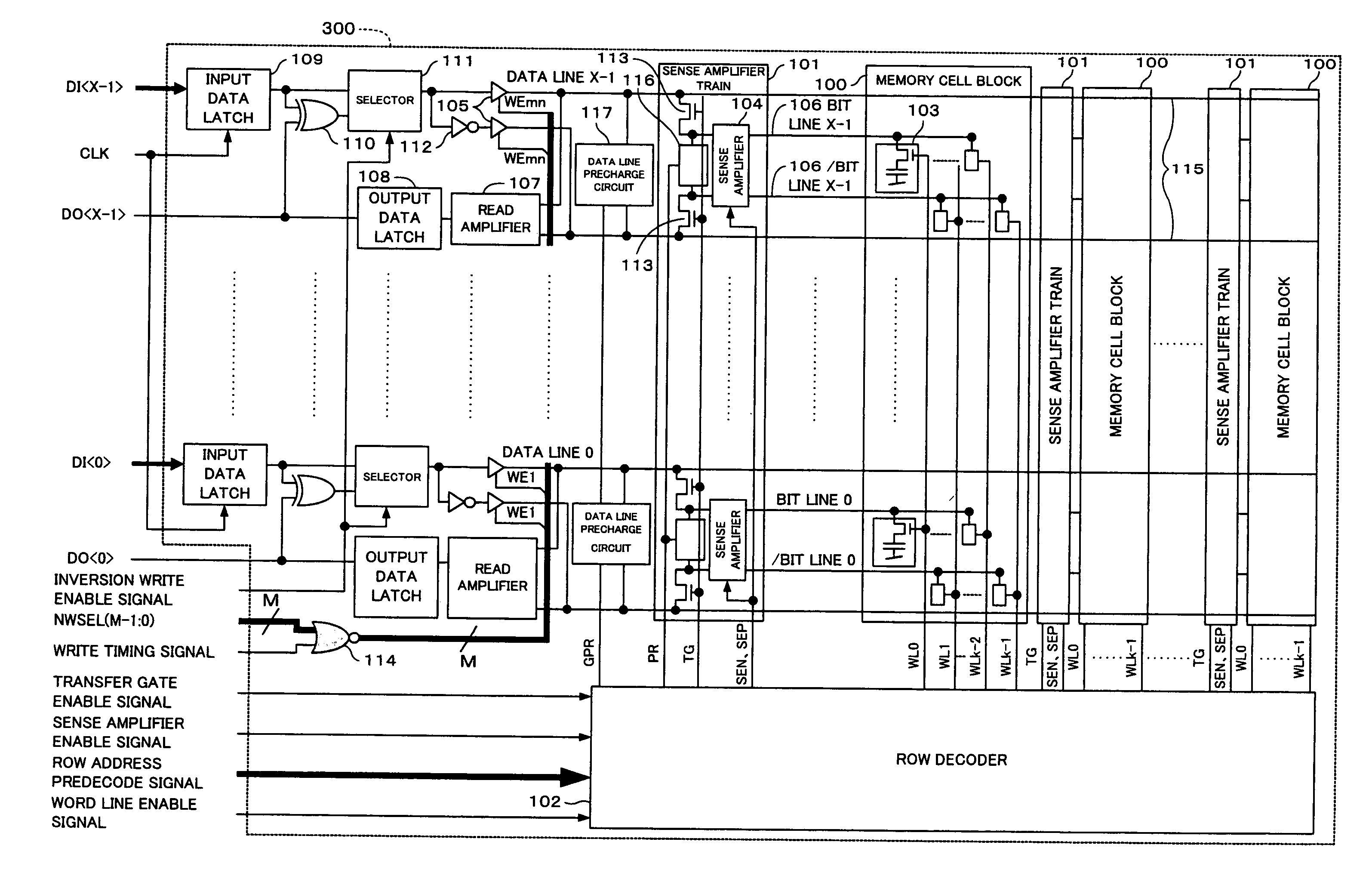
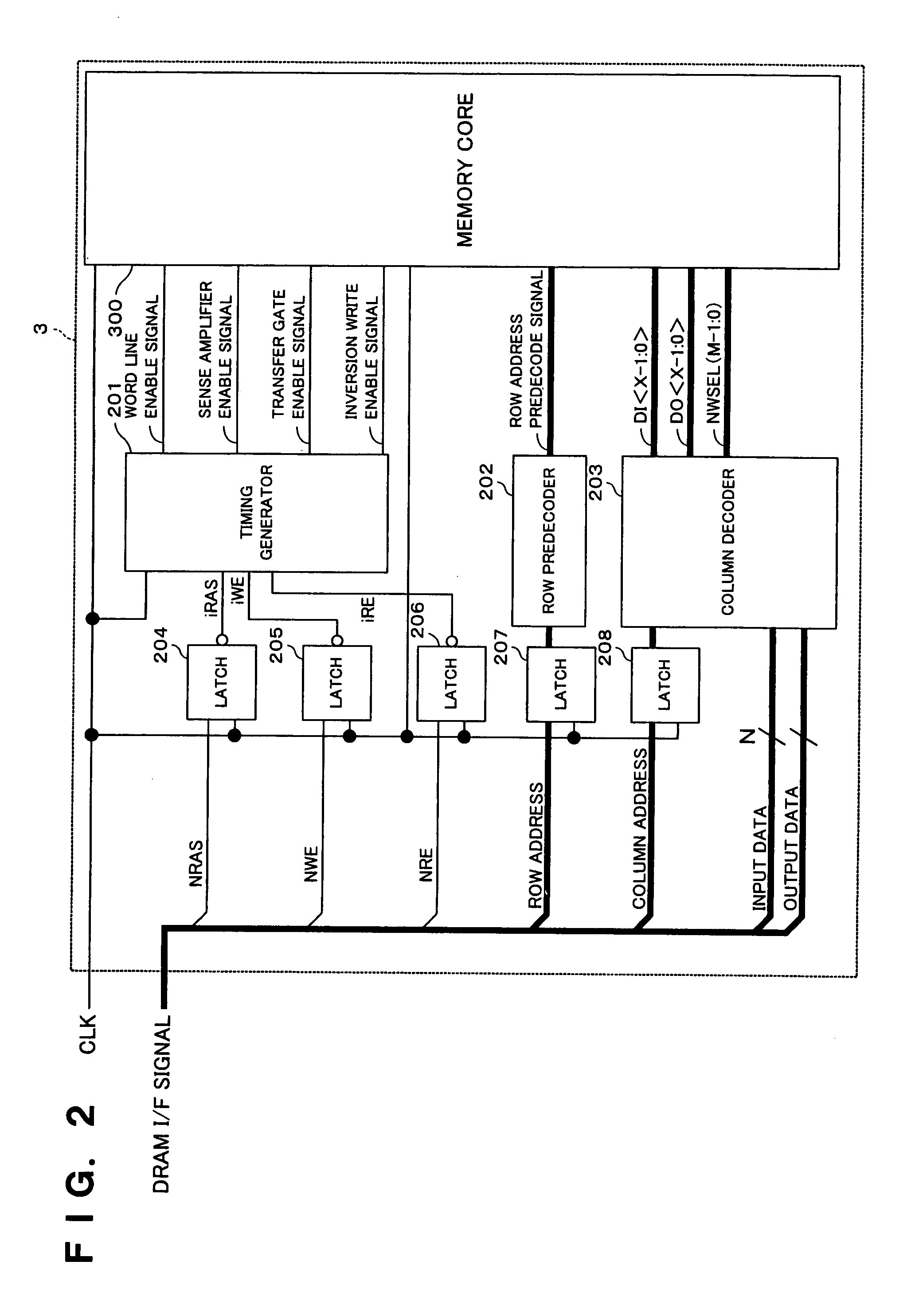
[0044]FIG. 2 is a circuit block diagram showing the memory 3. As shown in FIG. 2, the memory 3 include...

second embodiment

[0096]Next, description will be given of a semiconductor memory according to a second embodiment of the present invention.

[0097]FIG. 11 is a block diagram showing a configuration of the semiconductor memory according to the second embodiment. As shown in FIG. 11, in addition to the components of the memory 3 according to the first embodiment, the memory 3 according to the second embodiment includes an output data inversion latch circuit 1101 and receives an inversion control signal NEXOR. Specifically, the output data inversion latch circuit 1101 has an input end for receiving an inversion control signal NEXOR, and an output end for outputting an inversion write enable signal as output data.

[0098]With this configuration, one control terminal is additionally provided as compared with the configuration in the first embodiment. However, the memory 3 can directly receive an inversion write enable signal from an external unit. Thus, if it is obvious that desired data is prepared at an ou...


PUM

PropertyMeasurementUnit
standby timeaaaaaaaaaa
speedaaaaaaaaaa
timeaaaaaaaaaa

Abstract

In order to correct an error in input data to thereby obtain write data, in a memory core, an EXOR element performs arithmetic processing based on an output result of an output data latch for latching read data and a result of inputted array input data, and a selector selects a result of the arithmetic processing to prepare write data. Thus, data obtained after performance of the arithmetic processing can be generated in a semiconductor memory by an operation performed immediately after data read. In addition, it is unnecessary to transfer data to an external logic circuit. Therefore, the result of the arithmetic processing can be written to a memory cell block in a subsequent clock.

Description

BACKGROUND OF THE INVENTION[0001](1) Field of the Invention[0002]The present invention relates to a semiconductor memory which is mounted on a semiconductor device formed on a semiconductor substrate and stores data obtained by arithmetic processing or the like.[0003](2) Description of the Related Art[0004]With reference to the drawings, hereinafter, description will be given of a conventional semiconductor memory for storing data obtained by arithmetic processing or the like in a semiconductor device.[0005]FIG. 12 is a block diagram showing a configuration of the semiconductor device on which the conventional semiconductor memory is mounted. As shown in FIG. 12, the semiconductor device 1 includes a functional block 2, the semiconductor memory (hereinafter, simply referred to as “memory”) 3 having a function of storing data, an analog-to-digital (hereinafter, abbreviated as “A / D”) converter 4, a logic circuit 5, and a pad 6.[0006]Specifically, the semiconductor device 1 is configur...

Claims


Application Information

Patent Timeline
Patent Type & Authority Patents(United States)
IPC IPC(8): G06F11/00G06F11/08G11B20/18
CPCG11C7/1006G11C7/1078G11C7/1087G11C2029/0411
Inventor ORIGASA, KENICHIOHTA, KIYOTO
Owner PANASONIC SEMICON SOLUTIONS CO LTD
Why Eureka
Try Eureka