Wafer level processing for backside illuminated sensors

a backside illumination and sensor technology, applied in the field of wafer level can solve the problems of insufficiently addressed conventional techniques, adversely affecting the fill factor and quantum efficiency of image sensors, and difficult processing of backside illumination image sensors, etc., to achieve improved image quality, increase the size or cost of image sensors, and improve the performance of such devices

Active Publication Date: 2010-12-28
OMNIVISION TECH INC
View PDF10 Cites 120 Cited by
  • Summary
  • Abstract
  • Description
  • Claims
  • Application Information

AI Technical Summary

Benefits of technology

[0009]Illustrative embodiments of the invention provide backside illuminated image sensors that are easier to process, and exhibit improved performance relative to conventional sensors.
[0014]A backside illuminated image sensor in accordance with the invention may be advantageously implemented in a digital camera or other type of imaging device, and provides improved performance in such a device without significantly increasing image sensor die size or cost. For example, use of a transparent image sensor cover with a central cavity and peripheral supports provides better image quality than conventional arrangements. Also, the illustrative embodiments overcome the drawbacks of conventional techniques with regard to use and attachment of temporary carrier wafers, and formation of interconnects between image sensor bond pads and solder balls or other package contacts.

Problems solved by technology

However, the presence of metallization level interconnects and various other features associated with the dielectric layers on the frontside of the image sensor can adversely impact the fill factor and quantum efficiency of the image sensor.
Backside illuminated image sensors can be difficult to process due to the thinning or removal of the silicon substrate.
Important processing issues that are not adequately addressed by conventional techniques include use and attachment of temporary carrier wafers, proper configuration and placement of image sensor covers for optimum image quality, and formation of interconnects between image sensor bond pads and solder balls or other package contacts.
Accordingly, certain conventional processing techniques, such as those disclosed in, for example, U.S. Patent Application Publication No. 2007 / 0194397, entitled “Photo-Sensor and Pixel Array with Backside Illumination and Method of Forming the Photo-Sensor,” can suffer from increased die size, higher cost, and decreased image quality.

Method used


Image

  • Wafer level processing for backside illuminated sensors
  • Wafer level processing for backside illuminated sensors
  • Wafer level processing for backside illuminated sensors

Examples


Embodiment Construction

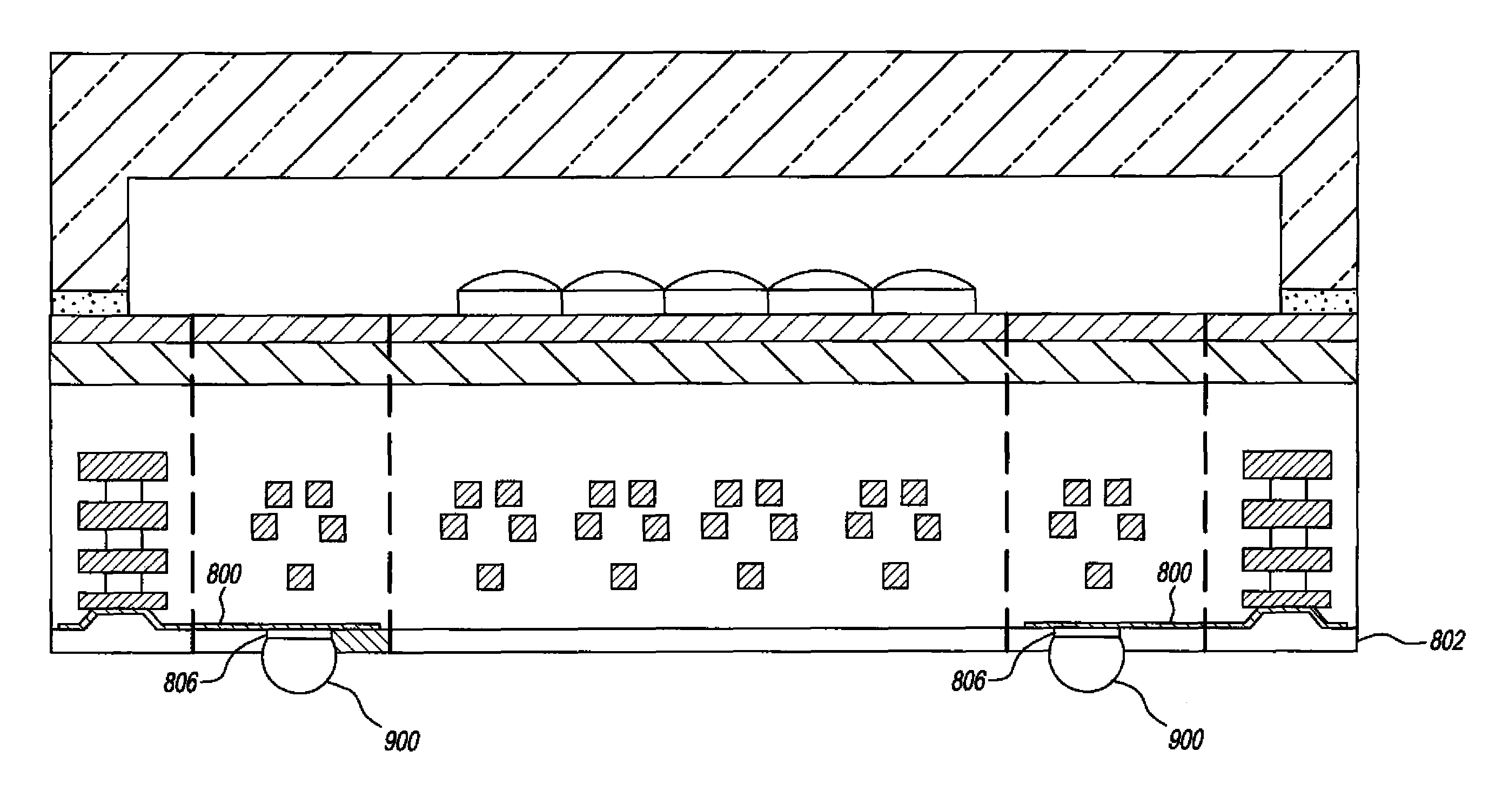
[0019]The present invention will be illustrated herein in conjunction with particular embodiments of digital cameras, backside illuminated image sensors, and processing techniques for forming such image sensors. It should be understood, however, that these illustrative arrangements are presented by way of example only, and should not be viewed as limiting the scope of the invention in any way. Those skilled in the art will recognize that the disclosed arrangements can be adapted in a straightforward manner for use with a wide variety of other types of imaging devices and image sensors.

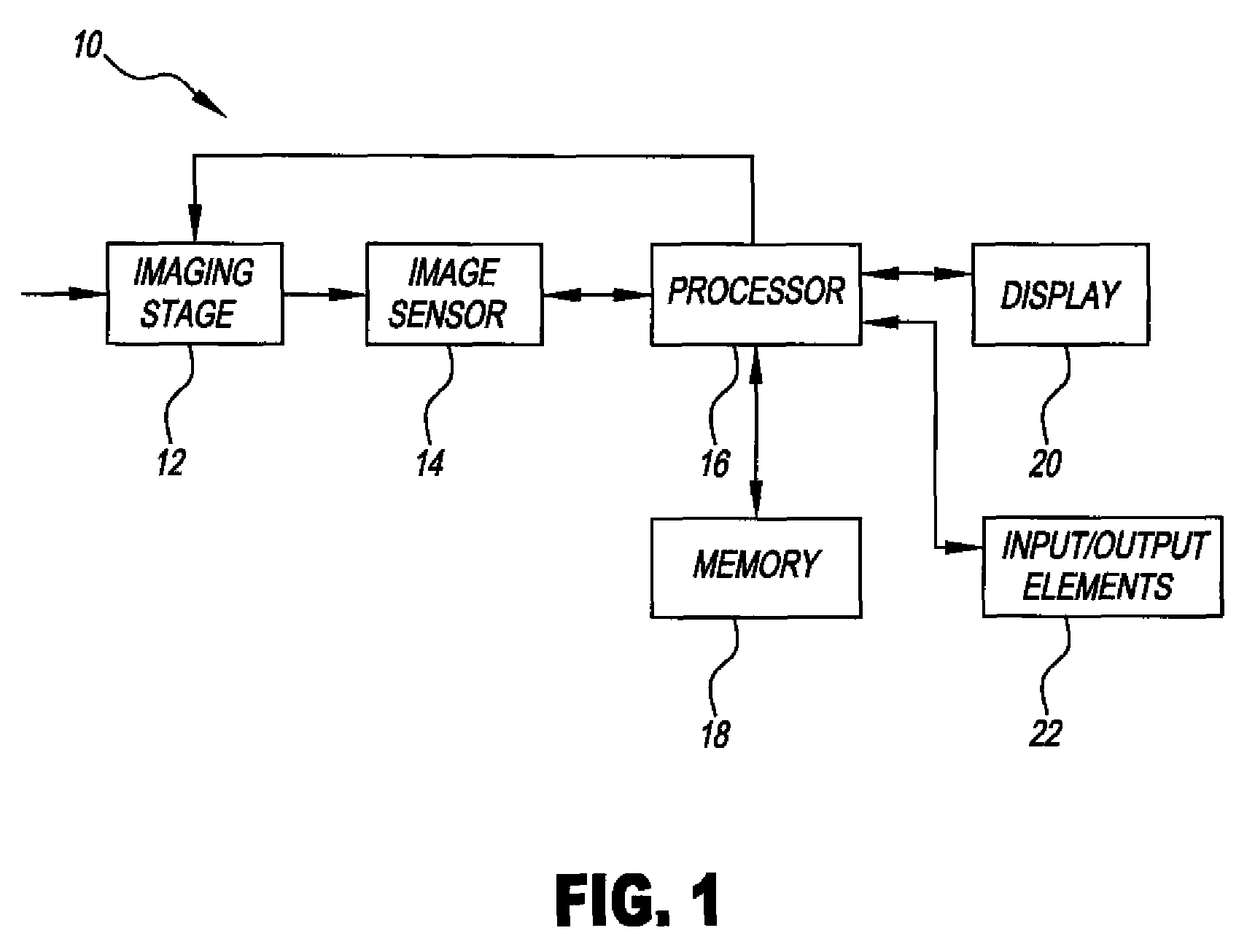
[0020]FIG. 1 shows a digital camera 10 in an illustrative embodiment of the invention. In the digital camera, light from a subject scene is input to an imaging stage 12. The imaging stage may comprise conventional elements such as a lens, a neutral density filter, an iris and a shutter. The light is focused by the imaging stage 12 to form an image on an image sensor 14, which converts the incident ligh...


PUM


Abstract

A backside illuminated image sensor comprises a sensor layer having a plurality of photosensitive elements of a pixel array, an oxide layer adjacent a backside surface of the sensor layer, and at least one dielectric layer adjacent a frontside surface of the sensor layer. A color filter array is formed on a backside surface of the oxide layer, and a transparent cover is attached to the backside surface of the oxide layer overlying the color filter array. Redistribution metal conductors are in electrical contact with respective bond pad conductors through respective openings in the dielectric layer. A redistribution passivation layer is formed over the redistribution metal conductors, and contact metallizations are in electrical contact with respective ones of the respective redistribution metal conductors through respective openings in the redistribution passivation layer. The image sensor may be implemented in a digital camera or other type of digital imaging device.

Description

CROSS REFERENCE TO RELATED APPLICATIONS[0001]The present invention is related to the inventions described in commonly-assigned U.S. patent applications Ser. No. 12 / 169790, entitled “Color Filter Array Alignment Mark Formation in Backside Illuminated Image Sensors,” Ser. No. 12 / 169,810, entitled “Backside Illuminated Image Sensor with Shallow Backside Trench for Photodiode Isolation,” and Ser. No. 12 / 169,723, entitled “Backside Illuminated Image Sensor with Reduced Dark Current,” which are concurrently filed herewith. The disclosures of these related applications are incorporated by reference herein in their entirety.FIELD OF THE INVENTION[0002]The present invention relates generally to electronic image sensors for use in digital cameras and other types of imaging devices, and more particularly to processing techniques for use in forming backside illuminated image sensors.BACKGROUND OF THE INVENTION[0003]A typical electronic image sensor comprises a number of light sensitive picture ...

Claims


Application Information

Patent Timeline
Patent Type & Authority Patents(United States)
IPC IPC(8): H01L31/062
CPCH01L27/14618H01L27/1464H01L27/14683H01L27/14636H01L27/14627H01L2924/0002H01L2924/00
Inventor BRADY, FREDERICK T.
Owner OMNIVISION TECH INC
Why Eureka
Try Eureka