Laser diode
a laser diode and diode technology, applied in the field of laser diodes, can solve problems such as catastrophic optical mirror damage (comd) and achieve the effect of equal refractive index and equal refractive index
- Summary
- Abstract
- Description
- Claims
- Application Information
AI Technical Summary
Benefits of technology
Problems solved by technology
Method used
Image

Examples
first embodiment
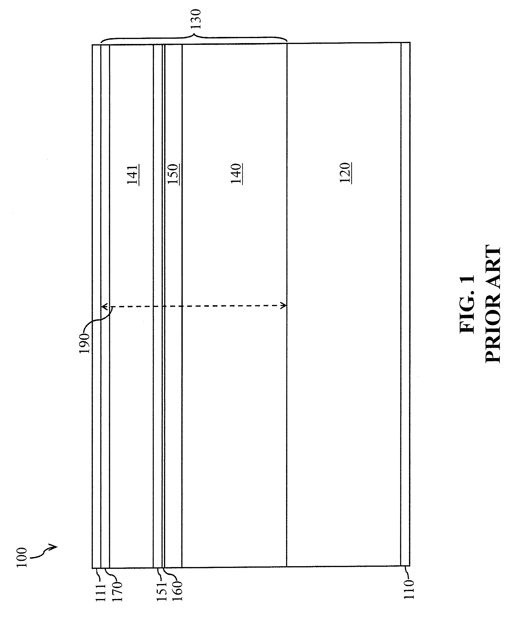
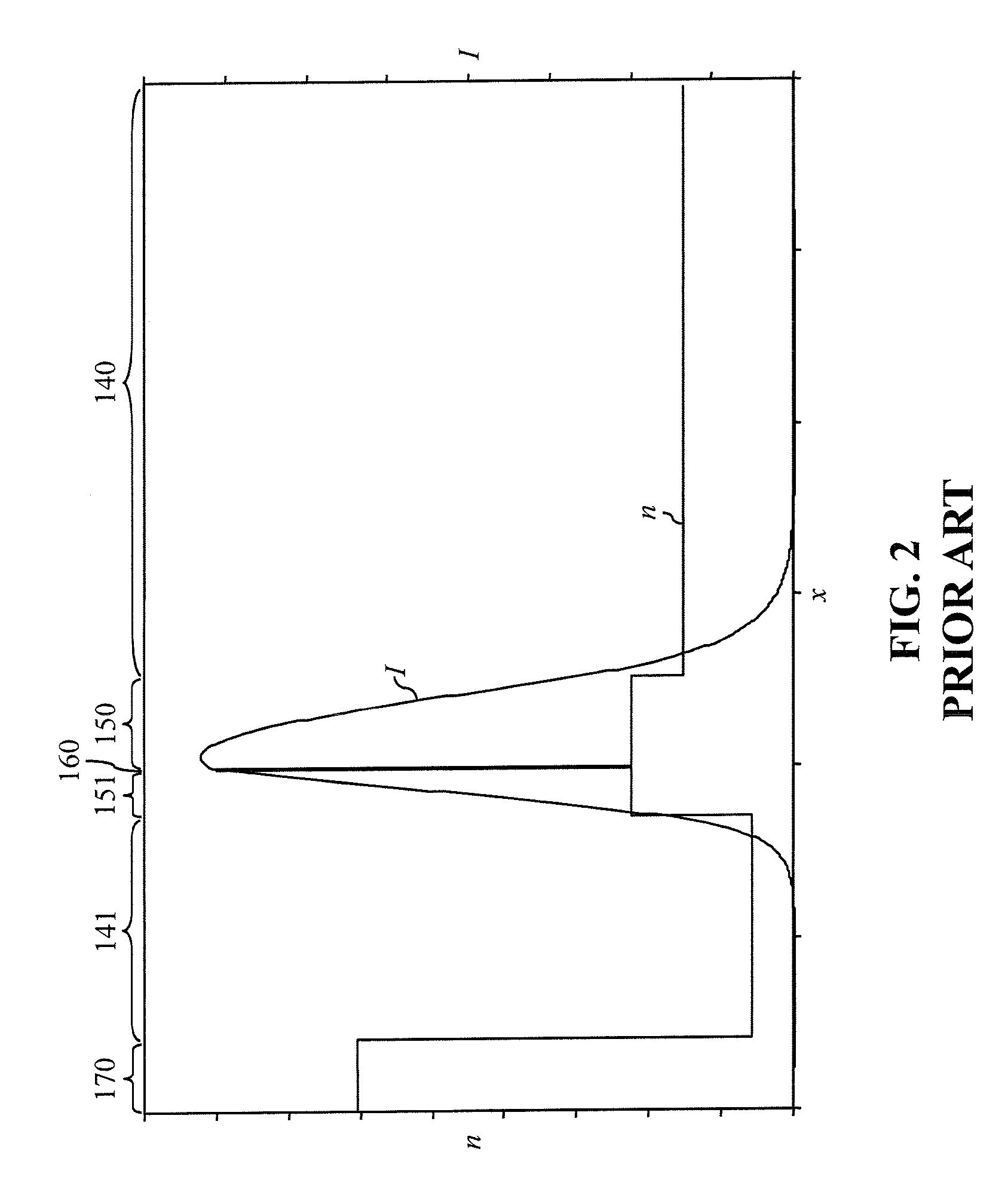
[0032]With reference to FIG. 5, a laser diode 500 according to the present invention has an asymmetric separate-confinement structure similar to that of the prior-art laser diode 100. The laser diode 500, typically, comprises a first metal layer 510 and a second metal layer 511 of metallic material, for passing current to or from the laser diode 500, as well as a substrate 520 and a layer stack 530 of semiconductor material.
[0033]Typically, the first metal layer 510 is disposed on a bottom surface of the substrate 520, and the second metal layer 511 is disposed on a top surface of the layer stack 530. The first metal layer 510 and the second metal layer 511 are, preferably, of one or more metals or metal alloys.
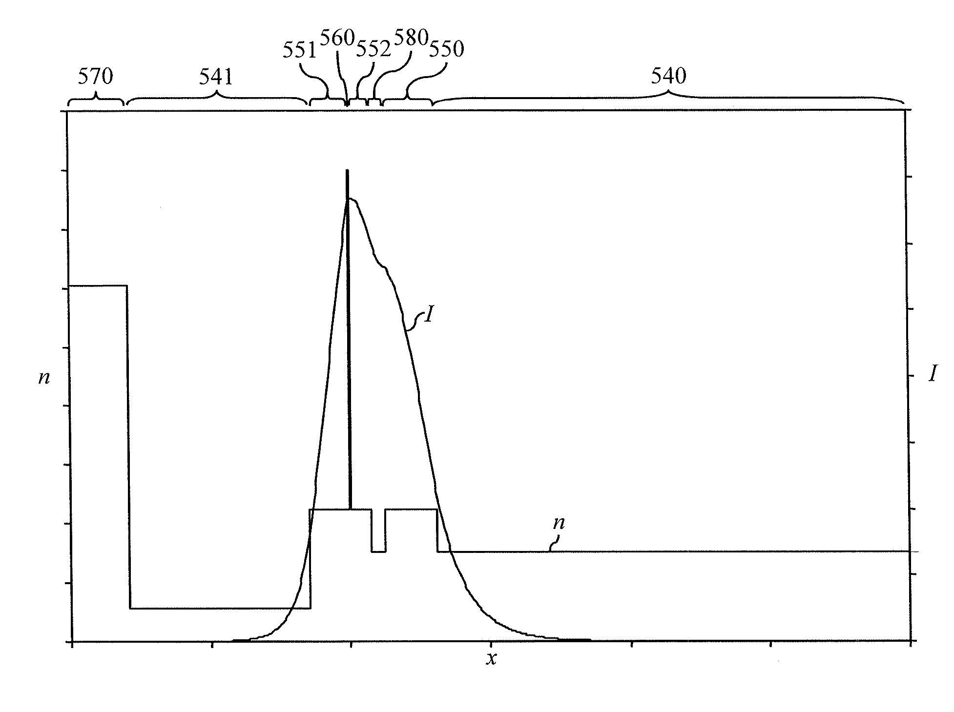
[0034]Preferably, the layer stack 530 is disposed on a top surface of the substrate 520. The layer stack 530 includes, in succession, a first cladding layer 540, for confining an optical mode, a first waveguide layer 550, for propagating the optical mode, a mode-splitting lay...
second embodiment
[0052]With reference to FIG. 7, a laser diode 700 according to the present invention comprises a layer stack 730 including a mode-splitting layer 780 that has a thickness that is two times the thickness of the mode-splitting layer 580 of the laser diode 500. The layer stack 730 is otherwise similar to that of the laser diode 500.
[0053]In FIG. 8, refractive index n and optical-mode intensity I are each plotted as a function of distance x from the second metal layer 511 along a vertical axis 790 through the laser diode 700 of FIG. 7. Comparison of FIG. 8 with FIG. 6 reveals that, in the laser diode 700, the vertical intensity profile of the optical mode is wider than that in the laser diode 500, whereas vertical overlap of the optical mode with the active layer 560 in the laser diode 700 is only slightly decreased relative to that in the laser diode 500. Thus, the increased thickness of the mode-splitting layer 780 leads to an increased vertical near-field beam width and a decreased v...
PUM
 Abstract
Description
Claims
Application Information
 - R&D
- Intellectual Property
- Life Sciences
- Materials
- Tech Scout
- Unparalleled Data Quality
- Higher Quality Content
- 60% Fewer Hallucinations
Browse by: Latest US Patents, China's latest patents, Technical Efficacy Thesaurus, Application Domain, Technology Topic, Popular Technical Reports.
© 2025 PatSnap. All rights reserved.Legal|Privacy policy|Modern Slavery Act Transparency Statement|Sitemap|About US| Contact US: help@patsnap.com