
Address-transparent device and method

a technology of address transparency and transparent devices, applied in the field of managing operations in semiconductor manufacturing, can solve the problems of long and demanding qualification cycles and standards for new equipment and modifications of old equipment, and the jitter in the time at which commands are initiated or completed is not well controlled in current software architectures, so as to achieve cost-effectiveness and avoid significant delays and fees

Active Publication Date: 2010-08-31
MKS INSTR INC
View PDF54 Cites 3 Cited by
  • Summary
  • Abstract
  • Description
  • Claims
  • Application Information

AI Technical Summary

Benefits of technology

The present invention is an address-transparent device that allows for communication between two networks in a semiconductor fab. The device can route packets between the two networks, regardless of the protocol used. It can also intercept packets for local use and reroute them to another destination by modifying the header of the original packet. Additionally, the invention provides a failsafe switch to ensure the device remains operational. The invention offers a cost-effective solution for adding services in a manufacturing environment without significant delays and fees associated in obtaining a new IP address for the newly inserted device. Overall, the invention allows for seamless communication between devices and sensors in a semiconductor fab.

Problems solved by technology

Because manufacturing batches are very valuable and manufacturing processes are sensitive to even small mistakes, semiconductor device manufacturing is a conservative business.
Qualification cycles and standards for new equipment and modifications of old equipment are lengthy and demanding.
Jitter in the time at which commands are initiated or completed is not well-controlled in current software architectures.

Method used


Image

  • Address-transparent device and method
  • Address-transparent device and method
  • Address-transparent device and method

Examples


Embodiment Construction

[0027]The SECS message protocols, communication infrastructure and hosting modes used by tools and other automated or semi-automated equipment in semiconductor fabs and foundries developed years ago, when communication and processor speeds were relatively limited. SECS message protocols for fab applications were designed to utilize low-speed, serial communications. These message protocols included structured messages, which could be transmitted quickly even with low-speed communications. Structured messages were and remain difficult to translate and understand. The difficulty is exacerbated when a first message sets a context for a response and a second, responsive message does not repeat the context; that is, the context-sensitive response is only meaningful when paired with the corresponding context-setting message. Communications typically were through RS 232 or equivalent serial communications, along dedicated channels, similar to modems and phone lines for terminals and time-sh...


PUM


Abstract

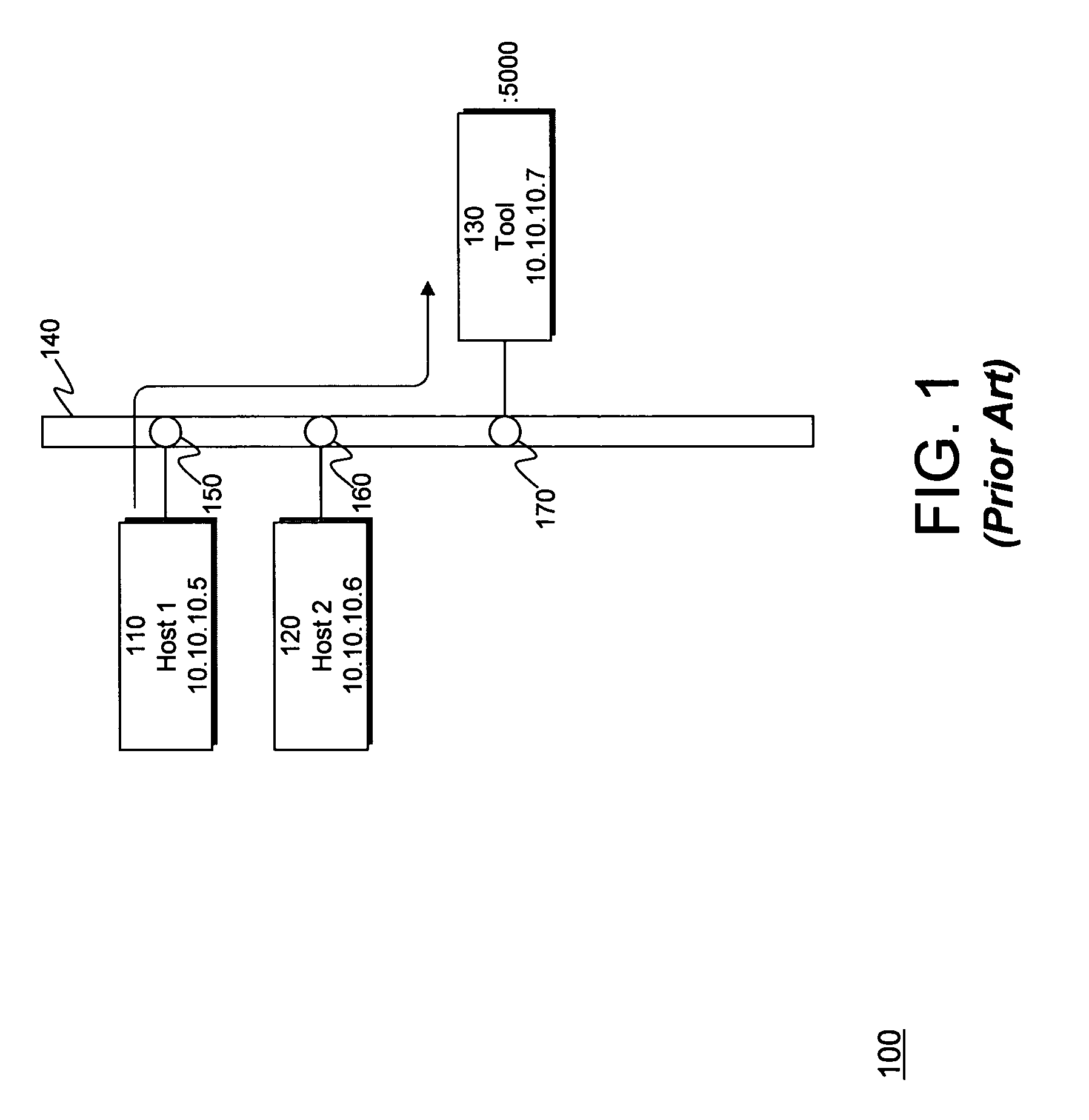
An address-transparent device is disclosed that couples two networks in a semiconductor fab and communicates packets between a host on a first network and a tool on a second network. Optionally, the address-transparent device intercepts packets for local use by a data consumer that resides within or outside of the address-transparent device. The address-transparent device can intercept all or a portion of data streams. As another option, the address-transparent device reroutes packet to another destination by changing the header of the received packet.

Description

CROSS REFERENCE TO RELATED APPLICATIONS[0001]This application relates to the co-pending U.S. Patent Application No. 60 / 591,286 entitled “Failsafe Switching of Intelligent Controller Method and Device”, by inventors Uzi Lev-Ami, Guenter Sifnatsch and Nidal Khalil, filed on 27 Jul. 2004; U.S. patent application Ser. No. 09 / 935,213 entitled “Method and Apparatus for Monitoring Host to Tool Communications,” by inventors Uzi Lev-Ami and Yossef Ilan Reich, filed on 22 Aug. 2001; and U.S. patent application Ser. No. 10 / 819,903, “Controller and Method to Mediate Data Collection from Smart Sensors for Fab Applications” by inventors Uzi Lev-Ami, Guenter Sifnatsch and Mark Attwood, filed on 7 Apr. 2004. Those co-pending applications are owned by the assignee of this application and incorporated by reference as if fully set forth herein.BACKGROUND OF THE INVENTION[0002]1. Field of the Invention[0003]The present invention relates generally to managing operations in semiconductor manufacturing, a...

Claims


Application Information

Patent Timeline
Patent Type & Authority Patents(United States)
IPC IPC(8): H04L12/28
CPCH04L29/12349H04L45/00H04L61/2507H04L29/12028H04L61/103H04L67/12H04L61/2503H04L45/54H01L21/00
Inventor SIFNATSCH, GUENTERRICHTER, MATTHEWMAKHOTA, MAXYM
Owner MKS INSTR INC
Learn More