Joining method and device produced by this method and joining unit
a technology of joining method and device, applied in the direction of instruments, soldering apparatus, semiconductor lasers, etc., can solve the problems of sudden bonding, achieve the effect of avoiding charge-up damage, reducing bonding load, and high profile irregularity
- Summary
- Abstract
- Description
- Claims
- Application Information
AI Technical Summary
Benefits of technology
Problems solved by technology
Method used
Image
Examples
first embodiment
[0164]Hereinafter, a first embodiment of the present invention will be described with reference to the drawings. FIG. 15 illustrates the first embodiment of a bonding apparatus according to the present invention. In this embodiment, an apparatus for bonding a chip 20 formed of a semiconductor (first object to be bonded) and a substrate 22 (second object to be bonded) will be described as an example. A bonding surface of the chip 20 has a metal electrode 20a which is an electrode and is formed of gold, and a bonding surface of the substrate 22 has a metal electrode 22a which is an electrode and is provided at a position which allows to face the metal electrode 20a of the chip. The metal electrode 20a of the chip and the metal electrode 22a of the substrate are bonded together by pressing.
[0165]The bonding apparatus roughly includes a bonding mechanism 27 including a vertical drive mechanism 25 and a head section 26, a mounting mechanism 28 including a stage 10 and a stage table 12, a...
second embodiment
[0171]Next, a second embodiment of the bonding apparatus of the present invention will be described in detail with reference to FIGS. 16A and 16B. This embodiment is significantly different from the above-described first embodiment in that a bonding portion of an object to be bonded is constructed by forming a gold film on a surface of a base material formed of a metal, and other parts of this embodiment are similar to those of the first embodiment. Hereinafter, the second embodiment will be described in detail, mainly in terms of the difference from the first embodiment. Note that the same configuration and operation as those of the first embodiment will not be described.
[0172]In the second embodiment, bonding portions of the chip 20 and the substrate 22 are formed as metal bumps as follows. Specifically, a plurality of coppers are used as base materials 20b and 22b, and gold films 20c and 22c are formed on surfaces of the base materials 20b and 22b. The metal bumps are subjected t...
third embodiment
[0174]Next, a third embodiment of the bonding apparatus of the present invention will be described in detail. This embodiment is significantly different from the above-described first and second embodiments in that minute irregularities are formed on a surface of a bonding portion, and other parts and operations of this embodiment are similar to those of the first and second embodiments, and will not be described. Hereinafter, specific features of this embodiment will be described in detail.
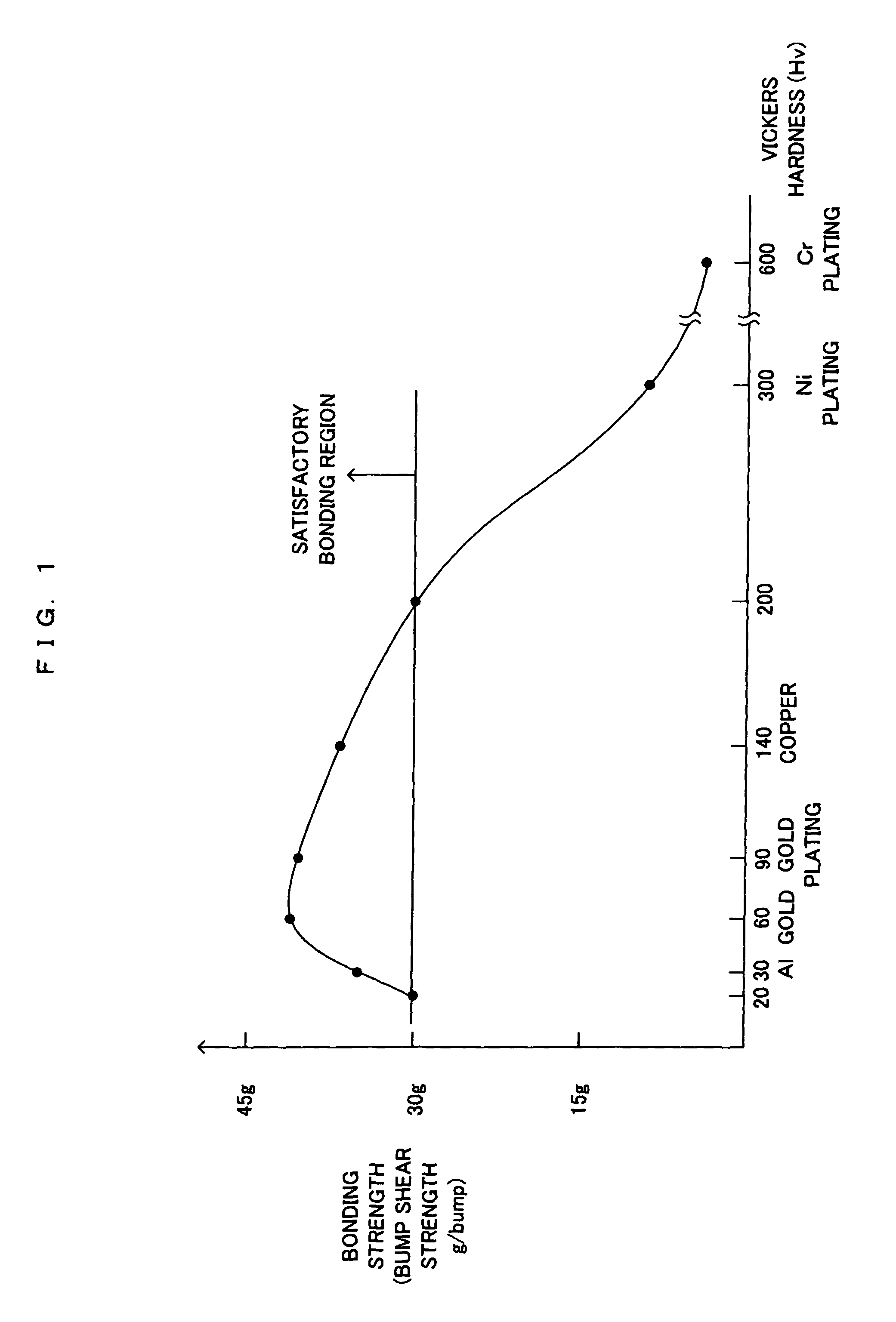
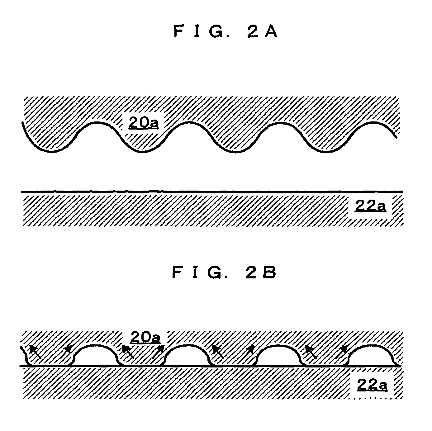
[0175]According to this embodiment, the convex portions are crushed by pressing when objects to be bonded are bonded as illustrated in FIGS. 2A and 2B and are then caused to be spread, so that a new surface appears and bonding is achieved. When viewed microscopically, crystal orientations arranged as illustrated in FIGS. 3A and 3B are rotated by the convex portion being crushed, so that the new surface appears. As can be seen from FIG. 4, when the surface roughness (minute irregularities) is 120 ...
PUM
| Property | Measurement | Unit |
|---|---|---|
| temperature | aaaaa | aaaaa |
| surface roughness | aaaaa | aaaaa |
| thickness | aaaaa | aaaaa |
Abstract
Description
Claims
Application Information
 - R&D
- Intellectual Property
- Life Sciences
- Materials
- Tech Scout
- Unparalleled Data Quality
- Higher Quality Content
- 60% Fewer Hallucinations
Browse by: Latest US Patents, China's latest patents, Technical Efficacy Thesaurus, Application Domain, Technology Topic, Popular Technical Reports.
© 2025 PatSnap. All rights reserved.Legal|Privacy policy|Modern Slavery Act Transparency Statement|Sitemap|About US| Contact US: help@patsnap.com


