Radiation-tolerant flash-based FPGA memory cells

a technology of flash-based fpga memory cells and flash-based gate arrays, which is applied in the field of flash-based fieldprogrammable gate arrays (fpga) integrated circuits, can solve the problems of damage to silicon dioxide, inability to tolerate, and compromise of the operation of the circuit programmed into the fpga

Active Publication Date: 2010-08-03
MICROSEMI SOC
View PDF15 Cites 13 Cited by
  • Summary
  • Abstract
  • Description
  • Claims
  • Application Information

AI Technical Summary

Problems solved by technology

Radiation due to heavy ions will damage the silicon dioxide either above or below the floating gate in a flash switch in a FPGA device.
This state change cannot be tolerated since it will cause unpredictable behavior in the programmed circuit that is configured in the FPGA.
In either case, the operation of the circuit programmed into the FPGA is compromised and the result is unpredictable, since there is no way to know which floating gate will be hit by a radiation event and whether the event will act to program or erase the affected floating gate.
In embodiments where a memory transistor and a switch transistor share a floating gate, the ability of stored charges to move freely between the memory and switch transistors is essential and the flash technologies with immobile control charges would not be suitable in such embodiments.
Thus standard transistors cannot have charge selectively added or removed to deliberately control the transistor threshold voltage.
While heavy ions can damage the gate oxide of a standard transistor, unless the damage is extremely severe (to the point where the gate gets shorted to the silicon substrate underneath the gate) the result is an undesirable but typically tolerable amount of gate leakage.
While gate leakage is catastrophic for a floating gate transistor since the floating gate is no longer isolated and charge can leak off changing the programming state, a standard transistor with a moderate amount of gate leakage will still continue to function like a standard transistor.

Method used


Image

  • Radiation-tolerant flash-based FPGA memory cells
  • Radiation-tolerant flash-based FPGA memory cells
  • Radiation-tolerant flash-based FPGA memory cells

Examples


Embodiment Construction

[0029]Persons of ordinary skill in the art will realize that the following description of the present invention is illustrative only and not in any way limiting. Other embodiments of the invention will readily suggest themselves to such skilled persons.

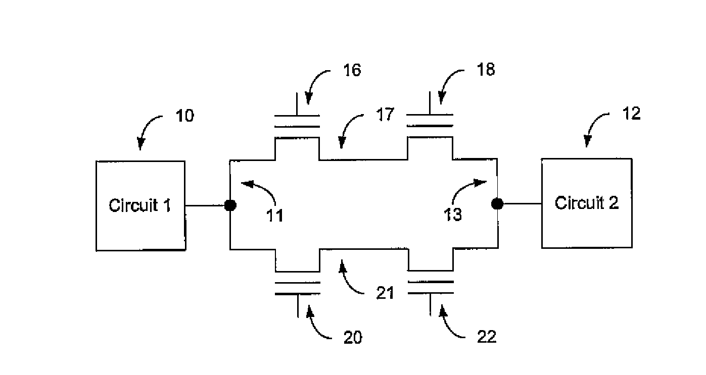
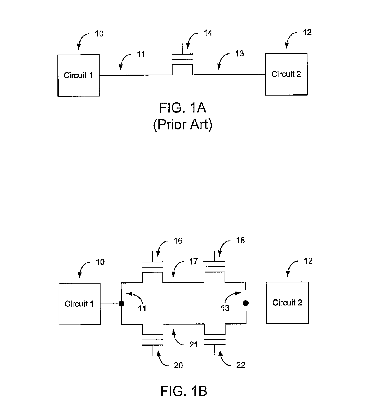
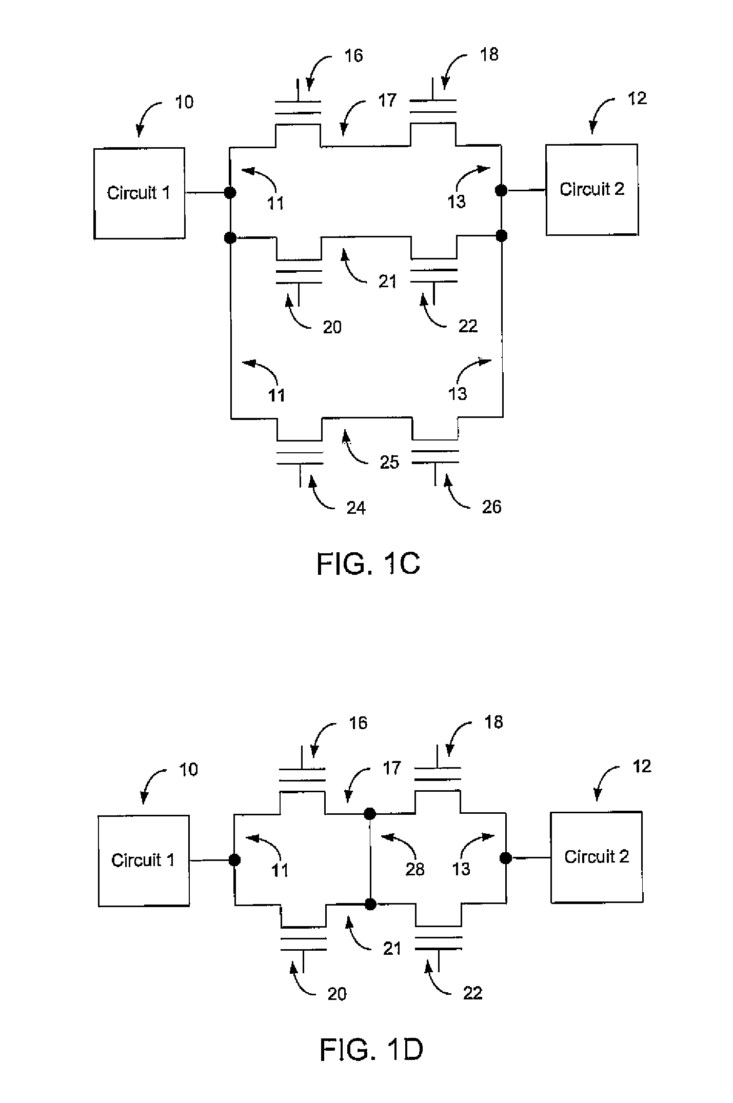
[0030]According to one aspect of the present invention, a radiation-tolerant flash-based FPGA switching element includes a plurality of memory cells each having a memory transistor and a switch transistor sharing a floating gate. The memory cells are combined in a series-parallel combination such that sets of switch transistors are wired in series and the sets of series-wired switch transistors are then wired in parallel. The four memory transistors associated with the series-parallel combination of switch transistors are all programmed to the same on or off state. The series combination prevents an “on” radiation-hit fault to one of the floating gates from creating a false connection and the parallel combination prevents an “off” rad...


PUM


Abstract

A radiation-tolerant flash-based FPGA switching element includes a plurality of memory cells each having a memory transistor and a switch transistor sharing a floating gate. Four such memory cells are combined such that two sets of two switch transistors are wired in series and the two sets of series-wired switch transistors are also wired in parallel. The four memory transistors associated with the series-parallel combination of switch transistors are all programmed to the same on or off state. The series combination prevents an “on” radiation-hit fault to one of the floating gates from creating a false connection and the parallel combination prevents an “off” radiation-hit fault to one of the floating gates from creating a false open circuit.

Description

BACKGROUND OF THE INVENTION[0001]1. Field of the Invention[0002]The Present invention relates to flash-based field-programmable gate array (FPGA) integrated circuits. More particularly, the present invention relates to a radiation-tolerant flash-based field-programmable gate array.[0003]2. The Prior Art[0004]Flash-based field-programmable gate array integrated circuits are known in the art. Such FPGAs use a flash switch including a floating gate memory transistor that shares a floating gate with a switch transistor that is used to make programmable connections between circuit nodes in the FPGA device. Both the memory transistor and the switch transistor are typically n-channel transistors. Radiation due to heavy ions will damage the silicon dioxide either above or below the floating gate in a flash switch in a FPGA device. Over time in a radiation environment, an increasing portion of the flash switches in the FPGA will be affected.[0005]A heavy ion passing through the silicon dioxi...

Claims


Application Information

Patent Timeline
Patent Type & Authority Patents(United States)
IPC IPC(8): H03K19/094
CPCG11C5/005G11C7/24G11C16/0441H03K19/00392
Inventor DHAOUI, FETHIWANG, ZHIGANGMCCOLLUM, JOHNCHAN, RICHARDBELLIPPADY, VIDYADHARA
Owner MICROSEMI SOC
Why Eureka
Try Eureka