
Solid-state imaging device, method for driving solid-state imaging device and camera

a solid-state imaging and imaging device technology, applied in the direction of radiation controlled devices, optical radiation measurement, instruments, etc., can solve the problems of undesirable saturation of pixels having high sensitivity, reduce the s/n ratio, etc., to prevent the reduction of the s/n ratio, reduce the sensitivity, and the effect of large signal

Active Publication Date: 2010-07-06
SONY SEMICON SOLUTIONS CORP
View PDF19 Cites 17 Cited by
  • Summary
  • Abstract
  • Description
  • Claims
  • Application Information

AI Technical Summary

Benefits of technology

[0008]Thus, it is desirable to achieve a wide dynamic range without reducing the S / N ratio of the pixels having low sensitivity and without saturating the pixels having high sensitivity.
[0011]According to the above embodiment of the invention, since different types of exposure time and readout timing can be applied to the first pixels and the second pixels with higher sensitivity than the first pixels, a long exposure time can be set to the first pixels having lower sensitivity than the second pixels so as to obtain a sufficiently large signal and hence prevent reduction in the S / N ratio, while a short exposure time can be set to the second pixels having higher sensitivity than the first pixels so as to prevent saturation. In this way, a wide dynamic range can be achieved.

Problems solved by technology

For example, when the exposure time is set such that the pixels having high sensitivity are not saturated, sufficient signal charge will not be obtained from the pixels having low sensitivity, resulting in a reduced S / N ratio.
On the other hand, when the exposure time is set such that sufficient signal charge will be obtained from the pixels having low sensitivity, the pixels having high sensitivity are undesirably saturated.

Method used


Image

  • Solid-state imaging device, method for driving solid-state imaging device and camera
  • Solid-state imaging device, method for driving solid-state imaging device and camera
  • Solid-state imaging device, method for driving solid-state imaging device and camera

Examples


Embodiment Construction

[0039]In the following description, “discrepancy” in exposure time means disagreement of the exposure timing between the low-sensitivity pixels and the high-sensitivity pixels in an arbitrary row, and “misalignment” of exposure time means the “discrepancy” varies depending on a readout row.

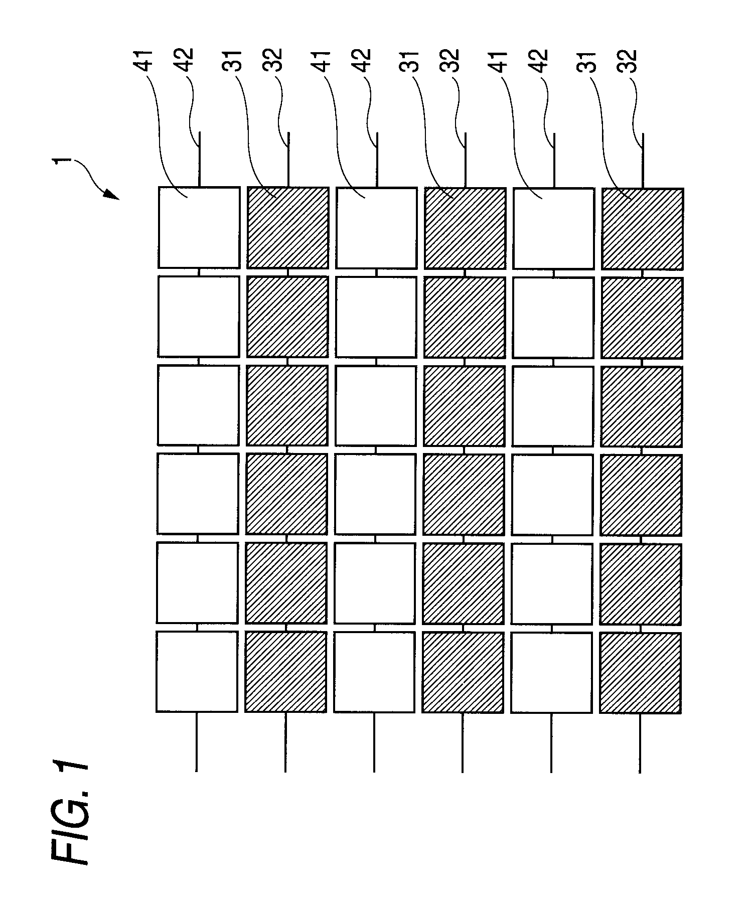
[0040]Firstly, an embodiment (first example) of the invention will be described with reference to the layout diagram shown in FIG. 1.

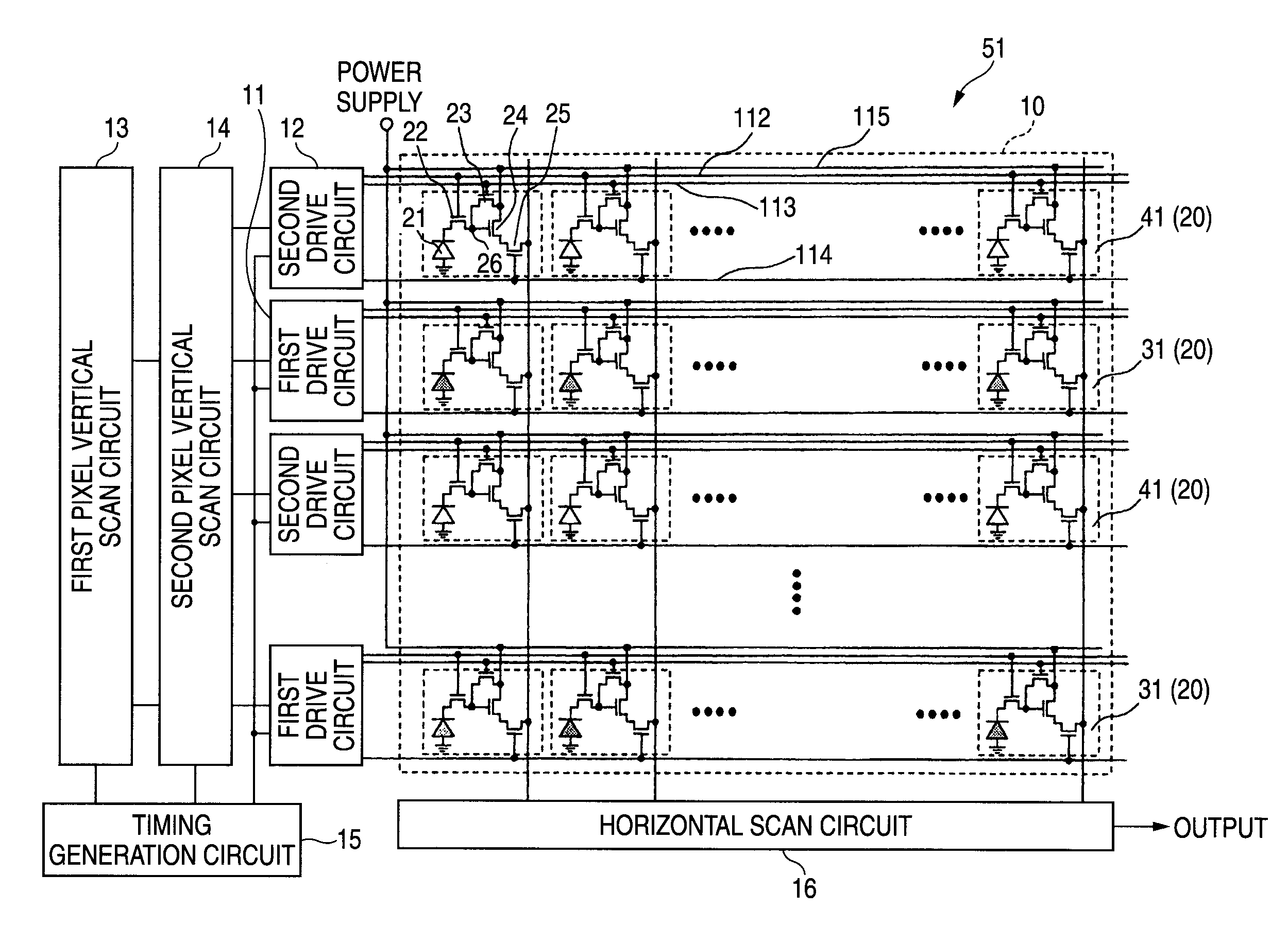
[0041]As shown in FIG. 1, a solid-state imaging device 1 has pixels arranged in a matrix two-dimensionally in the vertical direction (x direction) and the horizontal direction (y direction). There are first and second horizontal pixel rows alternately arranged in the vertical direction. The first pixel row is formed of a plurality of first pixels 31 arranged in the row direction and the second pixel row is formed of a plurality of second pixels 41, each having higher sensitivity than that of the first pixel 31, arranged in the row direction.

[0042]The first pixels 31 ...


PUM


Abstract

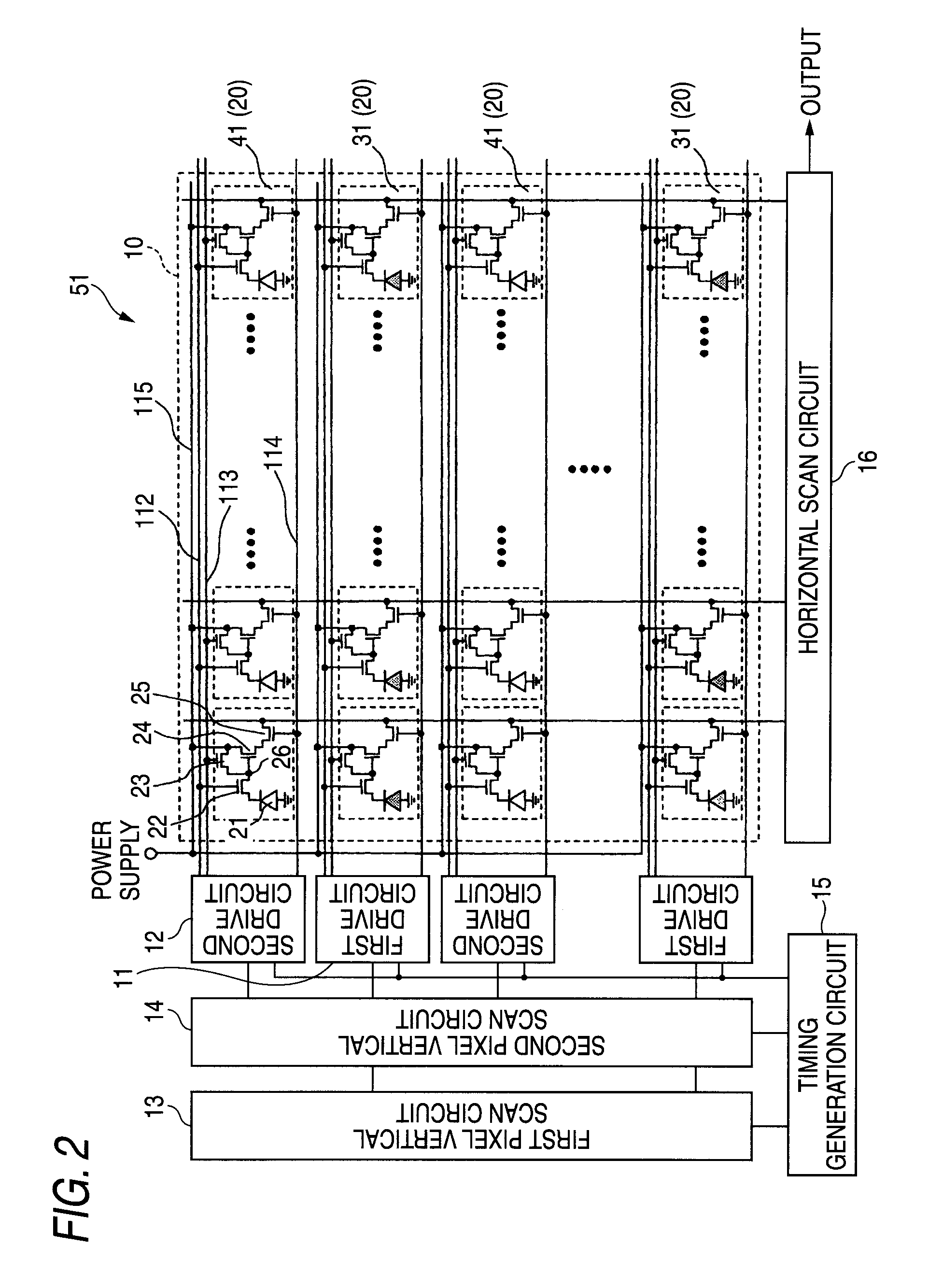
A solid-state imaging device including an array of a plurality of first pixels and a plurality of second pixels with higher sensitivity than the first pixels, a first control signal line that controls the first pixels, and a second control signal line that controls the second pixels, wherein the first control signal line and the second control signal line are driven independent of each other.

Description

CROSS REFERENCES TO RELATED APPLICATIONS[0001]The present invention contains subject matter related to Japanese Patent Application JP 2006-031932 filed in the Japanese Patent Office on Feb. 9, 2006, the entire contents of which being incorporated herein by reference.BACKGROUND OF THE INVENTION[0002]1. Field of the Invention[0003]The invention relates to a solid-state imaging device, a method for driving the solid-state imaging device and a camera.[0004]2. Description of the Related Art[0005]In a solid-state imaging device of related art, the same exposure time is applied to all pixels on the imaging plane. Even in the technology that enables a wide dynamic range by applying multiple numbers of exposure time in multiple imaging operations and integrating the resultant images (see JP-A-2004-363666, for example), the same exposure time is applied to all pixels. Thus, in a mixed pixel configuration in which some pixels have different sensitivity from the other, selection will be made in...

Claims


Application Information

Patent Timeline
Patent Type & Authority Patents(United States)
IPC IPC(8): H01L27/14H01L27/146H04N5/335H04N5/341H04N5/349H04N5/353H04N5/355H04N5/357H04N5/369H04N5/374H04N5/376H04N9/07
CPCH04N5/335H04N5/35554H04N25/585H04N25/583H04N25/00H01L27/146
Inventor OIKE, YUSUKEKASAI, MASANORIYOSHIMURA, SHINICHITODA, ATSUSHITAURA, TADAYUKISATO, HIROKI
Owner SONY SEMICON SOLUTIONS CORP
Learn More