Apparatus for epitaxially growing semiconductor device structures with sharp layer interfaces utilizing HVPE

a semiconductor device and epitaxial growth technology, applied in the direction of crystal growth process, polycrystalline material growth, chemically reactive gas, etc., can solve the problems of high electric field breakdown, direct band gap structure, high thermal conductivity, etc., to reduce gallium surface area, slow growth rate, and prevent thermal shock

Inactive Publication Date: 2010-03-02
OSTENDO TECH INC
View PDF84 Cites 12 Cited by
  • Summary
  • Abstract
  • Description
  • Claims
  • Application Information

AI Technical Summary

Benefits of technology

[0011]According to one aspect of the invention, a method and apparatus for fabricating multi-layer Group III nitride semiconductor devices in a single reactor run utilizing HVPE techniques is provided. Preferably an atmospheric, hot-walled horizontal furnace is used. Sources (Group III metals, Group V materials, acceptor impurities, donor impurities) are located within the multiple source zones of the furnace, the sources used being dependent upon the desired compositions of the individual layers. Preferably HCl is used to form the necessary halide metal compounds and an inert gas such as argon is used to transport the halide metal compounds to the growth zone where they react with ammonia gas. As a result of the reaction, epitaxial growth of the desired composition occurs. By controlling the inclusion of one or more acceptor impurity metals, the conductivity of each layer can be controlled.
[0013]In at least one embodiment of the invention, the reactor includes both a growth zone and a growth interruption zone. One or more gas inlet tubes direct a flow of gas (e.g., an inert gas) towards the growth interruption zone, thereby substantially preventing any reactive gases from entering into this zone. In use, after the growth of a layer is completed, the substrate is transferred from the growth zone to the growth interruption zone. The temperature of the substrate is maintained during the transfer and while the substrate is within the growth interruption zone, thus preventing thermal shock. While the substrate is within the growth interruption zone, the growth zone is purged and the sources required for the next desired layer are delivered to the growth zone. Once the reaction stabilizes, the substrate is returned to the growth zone. This process continues until all of the required device layers have been grown.
[0014]In at least one embodiment of the invention, the reactor uses a slow growth rate gallium source. The slow growth rate gallium source has a reduced gallium surface area. By reducing the surface area, there is less gallium available to react with the halide reactive gas. As a result, less gallium chloride is produced and fine control of the amount of gallium chloride delivered to the growth zone is possible.
[0015]In at least one embodiment of the invention, the reactor includes both a conventional gallium source and a slow growth rate gallium source. The slow growth rate gallium source dramatically reduces the surface area of the gallium exposed to the halide reactive gas, resulting in the production of less gallium chloride. Due to the low production levels, finer control of the amount of gallium chloride delivered to the growth zone is possible in contrast to the conventional source. Accordingly, a device can be fabricated during a single furnace run that includes both thick layers (i.e., utilizing the conventional gallium source) and thin layers (i.e., utilizing the slow growth rate gallium source).

Problems solved by technology

In particular, these materials exhibit a direct band gap structure, high electric field breakdown, and high thermal conductivity.
Although the MOCVD technique has proven adequate for a variety of commercial devices, the process has a number of limitations that constrain its usefulness.
First, due to the complexity of the various sources (e.g., trimethylaluminum, trimethylgallium, and biscyclopentiadienylmagnesium), the process can be very expensive and one which requires relatively complex equipment.
Second, the MOCVD technique does not provide for a growth rate of greater than a few microns per hour, thus requiring long growth runs.
The slow growth rate is especially problematic for device structures that require thick layers such as high voltage rectifier diodes that often have a base region thickness of approximately 30 microns.
Conventional HVPE techniques have been unable, however, to grow such layers.
As a result, the potential of the HVPE technique for fabricating devices based on Group III semiconductors has been limited.

Method used


Image

  • Apparatus for epitaxially growing semiconductor device structures with sharp layer interfaces utilizing HVPE
  • Apparatus for epitaxially growing semiconductor device structures with sharp layer interfaces utilizing HVPE
  • Apparatus for epitaxially growing semiconductor device structures with sharp layer interfaces utilizing HVPE

Examples


Embodiment Construction

[0027]The present invention provides a method and apparatus for producing submicron layers of III-V compounds utilizing HVPE techniques. As a result of the ability to fabricate such layers, the present invention allows a variety of device structures to be realized as well.

Processes

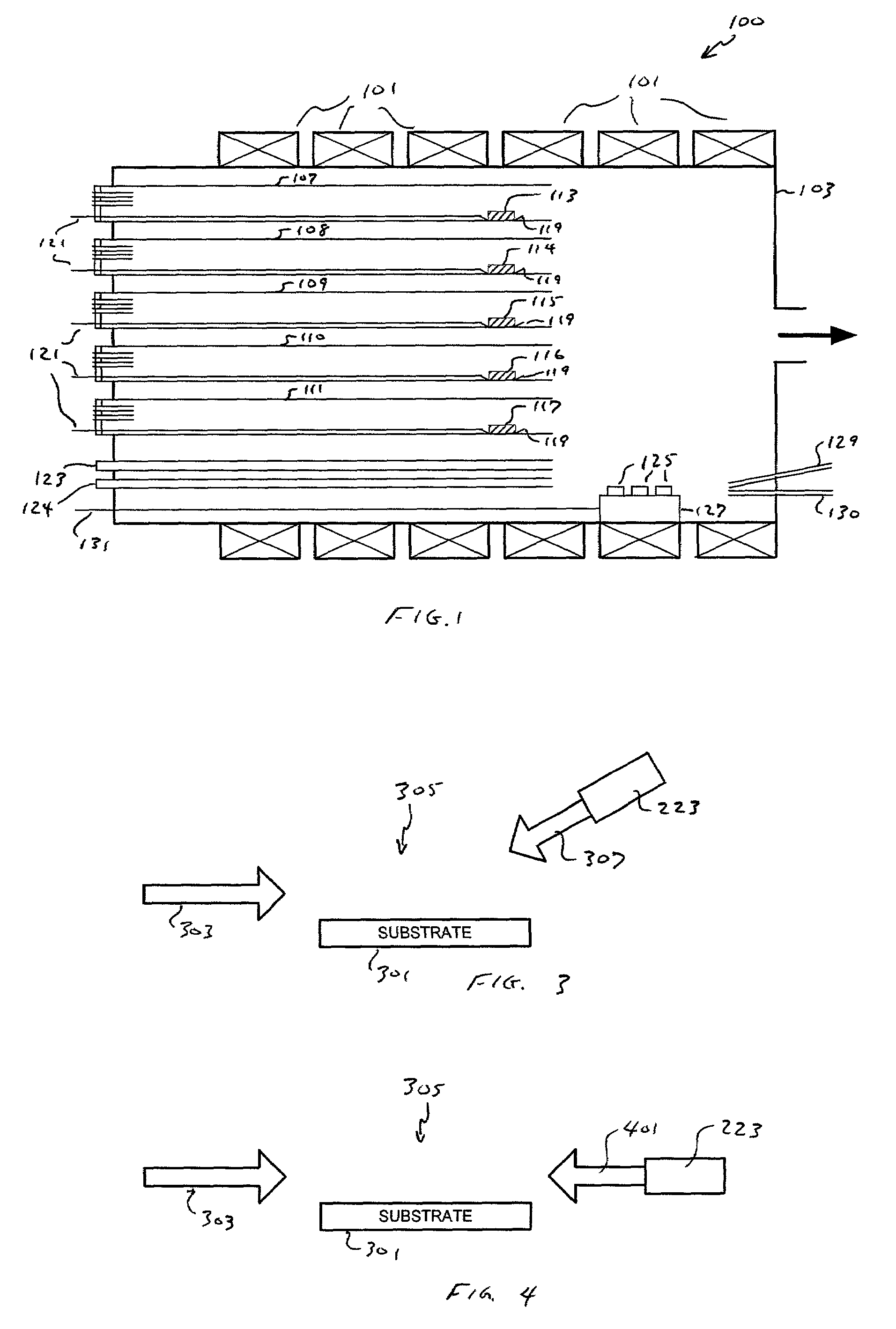
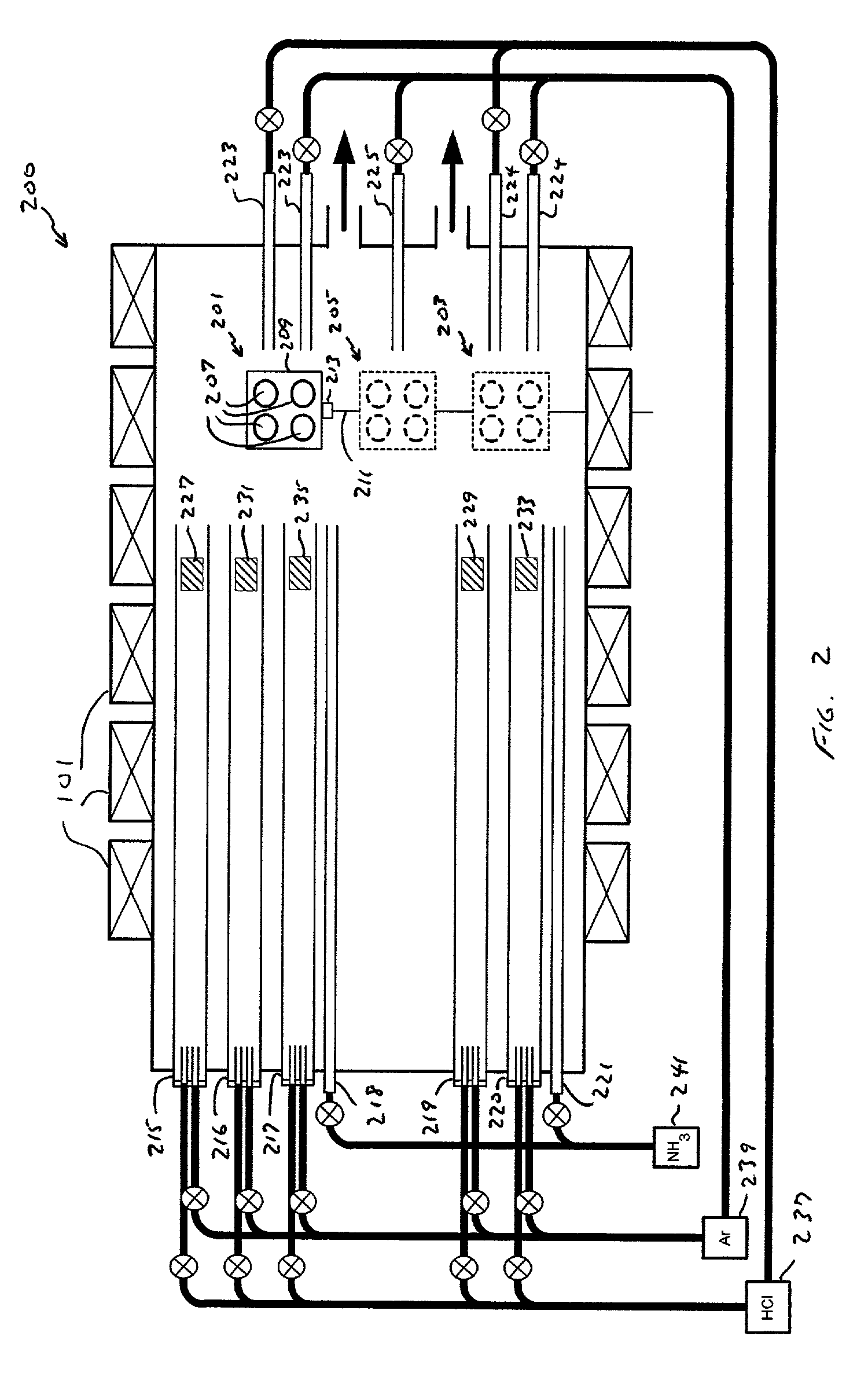
[0028]FIG. 1 is a schematic illustration of an atmospheric, hot-walled horizontal furnace 100 as used with the preferred embodiment of the invention. It should be understood that the invention is not limited to this particular furnace configuration as other furnace configurations (e.g., vertical furnaces) that offer the required control over the temperature, temperature zones, gas flow, source location, substrate location, etc., can also be used. Furnace 100 is comprised of multiple temperature zones, preferably obtained by using multiple resistive heaters 101, each of which at least partially surrounds furnace tube 103. It is understood that although reactor tube 103 preferably has a cylindrical cross-sec...


PUM

PropertyMeasurementUnit
temperatureaaaaaaaaaa
surface areaaaaaaaaaaa

Abstract

A method and apparatus for fabricating thin Group III nitride layers as well as Group III nitride layers that exhibit sharp layer-to-layer interfaces are provided. According to one aspect, an HVPE reactor includes one or more gas inlet tubes adjacent to the growth zone, thus allowing fine control of the delivery of reactive gases to the substrate surface. According to another aspect, an HVPE reactor includes both a growth zone and a growth interruption zone. According to another aspect, an HVPE reactor includes a slow growth rate gallium source, thus allowing thin layers to be grown. Using the slow growth rate gallium source in conjunction with a conventional gallium source allows a device structure to be fabricated during a single furnace run that includes both thick layers (i.e., utilizing the conventional gallium source) and thin layers (i.e., utilizing the slow growth rate gallium source).

Description

CROSS-REFERENCES TO RELATED APPLICATIONS[0001]This application claims priority from U.S. Patent Application Ser. Nos. 60 / 280,604 filed Mar. 30, 2001 and 60 / 283,743, filed Apr. 13, 2001, the disclosures of which are incorporated herein by reference for all purposes.FIELD OF THE INVENTION[0002]The present invention relates generally to semiconductor devices and, more particularly, to a method and apparatus for fabricating submicron layers of Group III nitride semiconductor materials.BACKGROUND OF THE INVENTION[0003]III-V compounds such as GaN, AlN, AlGaN, InGaN, InAlGaN, and InGaAlBNPAs have unique physical and electronic properties that make them ideal candidates for a variety of electronic and opto-electronic devices. In particular, these materials exhibit a direct band gap structure, high electric field breakdown, and high thermal conductivity. Additionally, materials such as InxAl1-xGaN can be used to cover a wide range of band gap energies, i.e., from 1.9 eV (where x equals 1) to...

Claims


Application Information

Patent Timeline
Patent Type & Authority Patents(United States)
IPC IPC(8): C23C16/00C30B25/02C30B25/08C30B25/14C30B25/16C30B29/40H01L21/205
CPCC23C16/303C23C16/4488C23C16/45514C30B25/02C30B25/08C30B25/14C30B25/16C30B29/40C30B29/403C30B29/406H01L21/0237H01L21/02458H01L21/02505H01L21/0254H01L21/02576H01L21/02579H01L21/0262H01L21/02631
Inventor TSVETKOV, DENIS V.NIKOLAEV, ANDREY E.DMITRIEV, VLADIMIR A.
Owner OSTENDO TECH INC
Why Eureka
Try Eureka