Image sensor with high fill factor pixels and method for forming an image sensor

a fill factor and image sensor technology, applied in the field of image sensor with high fill factor pixels and image sensor formation method, can solve the problems of limited area required for three or four readout elements for each pixel, higher power consumption and lower speed operation than cis devices, and achieve high fill factor and higher fill factor

Active Publication Date: 2010-02-23
SAMSUNG ELECTRONICS CO LTD
View PDF19 Cites 5 Cited by
  • Summary
  • Abstract
  • Description
  • Claims
  • Application Information

AI Technical Summary

Benefits of technology

[0008]The present invention is directed to an image sensor that provides the advantages of high-resolution image data with a high fill factor. This is accomplished, in part, by providing an image sensor that has shared-type pixel configuration, with photoelectric conversion elements that are arranged at a constant pitch in the row direction and at a constant pitch in the column direction. In this manner, microlens alignment is achieved, while obtaining a higher fill factor by utilizing the shared-type device configuration.

Problems solved by technology

CCD image sensors operate with low noise and with high uniformity, but generally require higher power consumption and lower speed operation than CIS devices.
However, further reduction of the area required for the three or four readout elements required for each pixel is limited, due to limitations in the minimization of the sizes of the transistor components of the readout elements, since noise increases with smaller element size.
Such a shared configuration is effective for improving the device fill factor; however, this shared configuration also introduces the problem of misalignment between microlenses formed on the devices, and corresponding photoelectric conversion elements.
Thus, misalignment occurs between the microlens array and the pixel array, degrading image quality.

Method used


Image

  • Image sensor with high fill factor pixels and method for forming an image sensor
  • Image sensor with high fill factor pixels and method for forming an image sensor
  • Image sensor with high fill factor pixels and method for forming an image sensor

Examples


Embodiment Construction

[0087]The present invention will now be described more fully hereinafter with reference to the accompanying drawings, in which preferred embodiments of the invention are shown. This invention may, however, be embodied in different forms and should not be construed as limited to the embodiments set forth herein. Like numbers refer to like elements throughout the specification.

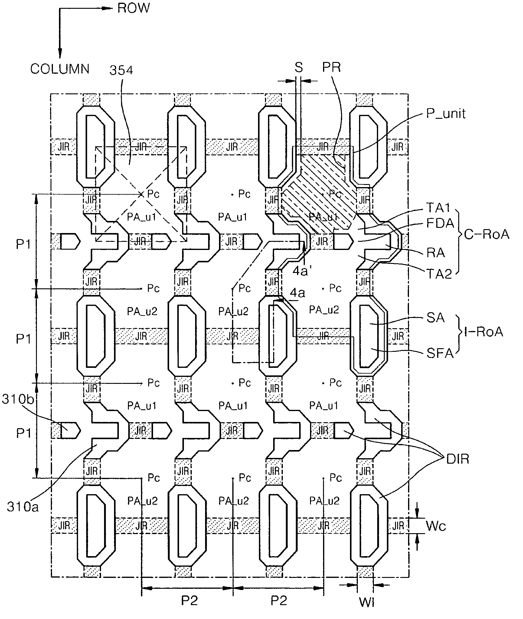
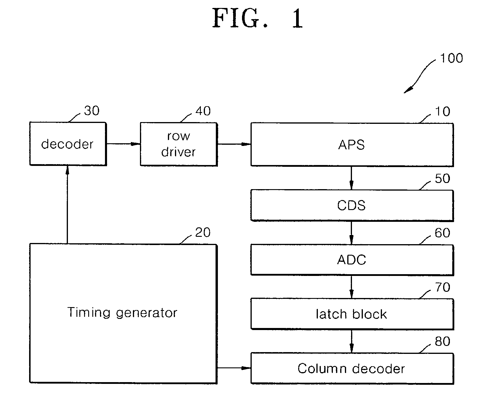
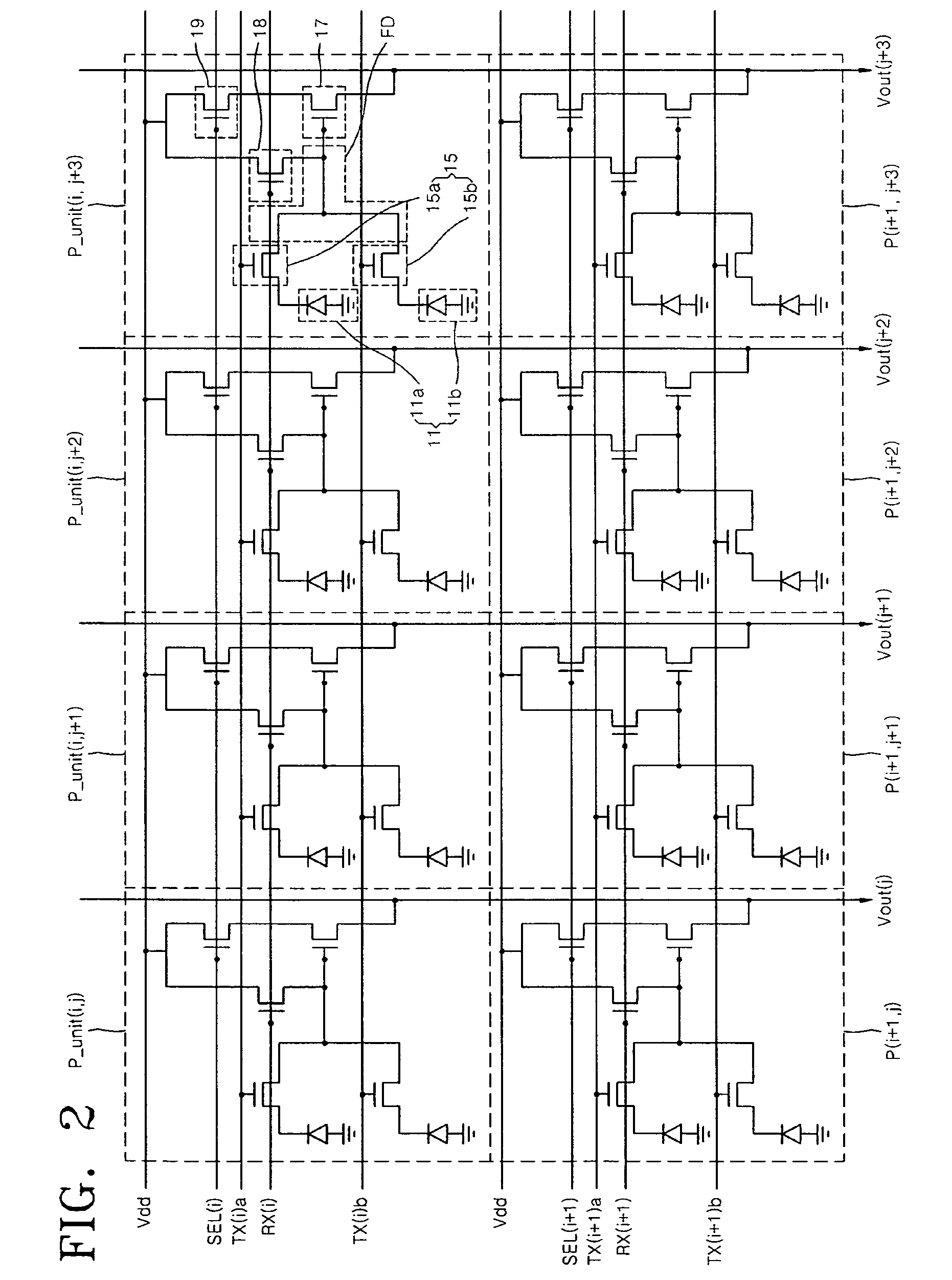
[0088]FIG. 1 is a block diagram of a CIS image sensor according to an embodiment of the present invention. Referring to FIG. 1, a CIS image sensor 100 includes an active pixel sensor array (APS) 10, a timing generator 20, a row decoder 30, a row driver 40, a correlated double sampler (CDS) unit 50, an analog to digital converter (ADC) 60, a latch block 70 and a column decoder 80. The APS 10 includes an array of individually addressable pixels, each including a photoelectric conversion element, and a plurality of readout elements. The readout elements include a transfer element, a select element, a driver element...


PUM


Abstract

An image sensor comprising an array of photoelectric conversion elements in a substrate, the photoelectric conversion elements being arranged in rows and columns extending in a first direction and a second direction respectively, a plurality of first junction isolation regions in the substrate that each isolate side portions of neighboring photoelectric conversion elements of a common row, and a plurality of second junction isolation regions in the substrate that each isolate side portions of neighboring photoelectric conversion elements of a common column, and a plurality of dielectric isolation regions in the substrate, that each isolate corner portions of neighboring photoelectric conversion elements. In one embodiment, the photoelectric conversion elements have a first pitch in the first direction and have a second pitch in the second direction and the first pitch is substantially equal for the photoelectric conversion elements of a common row, and the second pitch is substantially equal for the photoelectric conversion elements of a common column.

Description

RELATED APPLICATIONS[0001]This application is a continuation-in-part application of U.S. patent application Ser. No. 11 / 482,172, filed Jul. 7, 2006, and is a continuation-in-part application of U.S. patent application Ser. No. 11 / 481,733, filed Jul. 7, 2006, now U.S. Pat. No. 7,541,628 the content of each of which is incorporated herein by reference, in its entirety. This application further claims priority under 35 U.S.C. 119 to Korean Patent Application No. 10-2006-0022726 filed on Mar. 10, 2006, the content of which is incorporated herein by reference in its entirety.BACKGROUND OF THE INVENTION[0002]Semiconductor image sensing devices are widely used for capturing images in a variety of applications such as digital cameras, camcorders, printers, scanners, etc. Such devices include image sensors that capture optical information and convert the optical information into electrical signals, which are then processed, stored, and otherwise manipulated to result in projection of the cap...

Claims


Application Information

Patent Timeline
Patent Type & Authority Patents(United States)
IPC IPC(8): H01L31/00H01L27/14H04N5/335H04N5/369H04N5/374
CPCH01L27/14603H01L27/14641H01L27/14627
Inventor LEE, SEOK-HALEE, DUCK-HYUNGSHIN, JONG-CHEOLLEE, KANG-BOK
Owner SAMSUNG ELECTRONICS CO LTD
Why Eureka
Try Eureka