Apparatus for observing an assembled state of components and method of observing an assembled state of components using such apparatus
a technology for components and apparatus, applied in semiconductor/solid-state device testing/measurement, manufacturing tools, instruments, etc., can solve problems such as the inability to check the behavior of underfill resin
- Summary
- Abstract
- Description
- Claims
- Application Information
AI Technical Summary
Benefits of technology
Problems solved by technology
Method used
Image
Examples
first embodiment
[0031]Preferred embodiments of an apparatus for observing an assembled state of components will now be described with reference to the attached drawings.
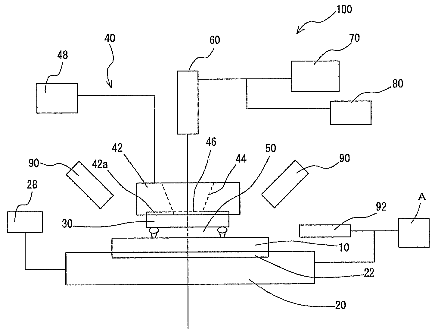
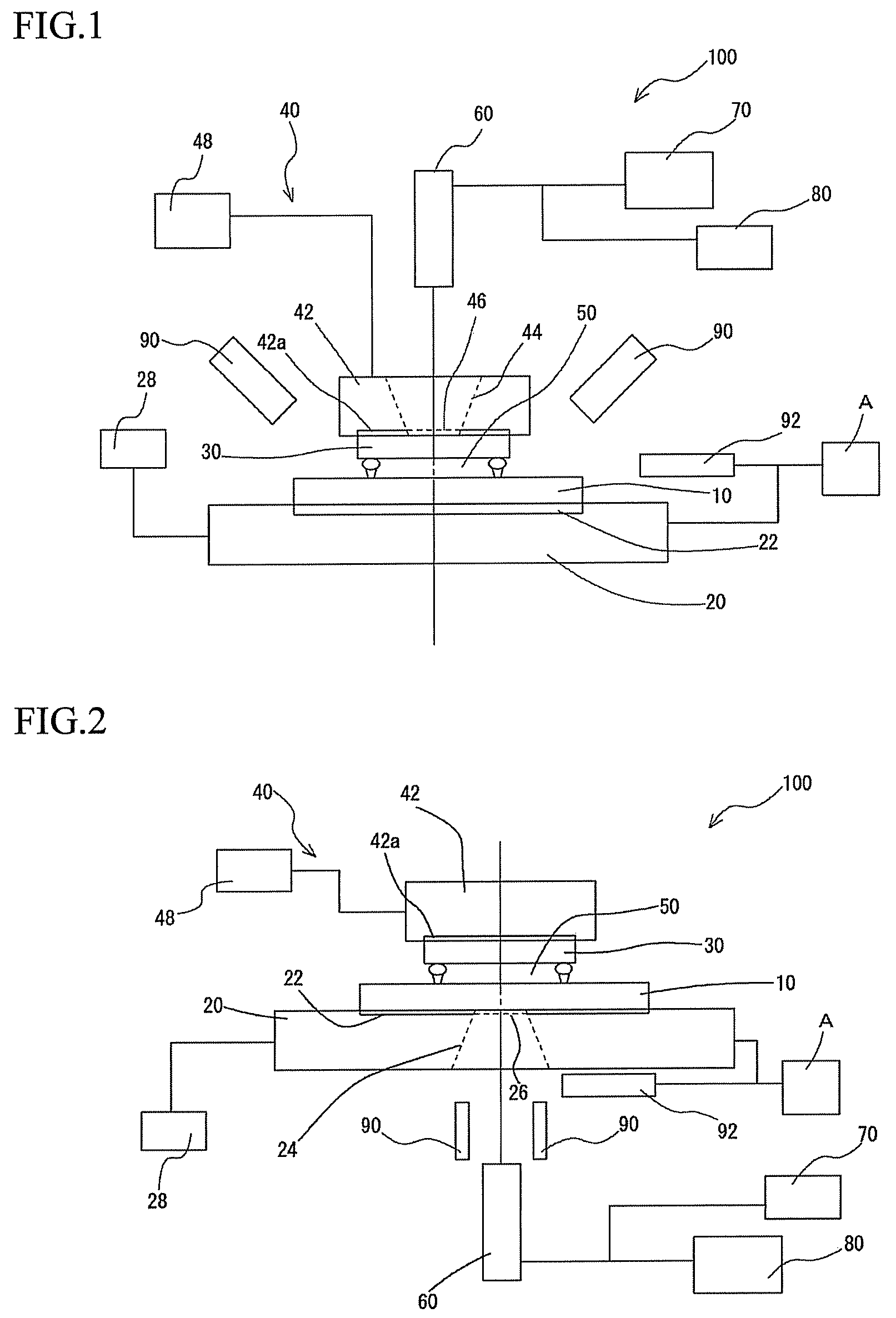
[0032]FIG. 1 is a schematic diagram showing the construction of an apparatus for observing an assembled state of components according to a first embodiment of the present invention.
[0033]The observing apparatus 100 for observing an assembled state of components according to the present embodiment includes a stage 20 on which a substrate 10 is set, a head mechanism 40 for supporting an observation workpiece 30 and bonding the observation workpiece 30 to the substrate 10, a camera 60 that takes images of the bonded state of the substrate 10 on the stage 20 and the observation workpiece 30, a display apparatus 70 that outputs the images taken by the camera 60, and a storage unit 80 that stores image data taken by the camera 60.
[0034]Note that in the present embodiment, resin 50 is supplied in advance onto the substrate 10 and in this s...
second embodiment
[0051]FIG. 2 is a schematic diagram showing the construction of an apparatus 100 for observing an assembled state of components according to a second embodiment of the present invention. The construction of the observing apparatus 100 for observing an assembled state of components according to the second embodiment is fundamentally the same as that of the first embodiment described earlier.
[0052]In the second embodiment, the substrate 10 is formed of a transparent material such as glass and the observing apparatus 100 is constructed so as to take images of the observed part from the substrate 10 side. By using this construction, it is possible to use the same workpiece (i.e., a semiconductor chip) as that actually mounted on a substrate 10 as the observation workpiece 30.
[0053]In the present embodiment, there is no need to form the imaging hole 44 that is formed in the pressing head 42 in the first embodiment. The camera 60 takes images of the observed part of the substrate 10 and t...
third embodiment
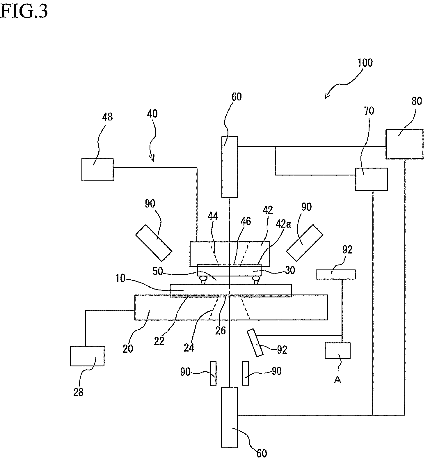
[0055]The present embodiment is a combination of the first embodiment and the second embodiment. That is, both the substrate 10 and the workpiece 30 are formed from a transparent material such as glass and images of the observed part are taken simultaneously from both the substrate side and the observation workpiece side (i.e., from both below and above) by a camera 60 disposed above the workpiece 30 (the stage 20) and a camera 60 disposed below the stage 20.
[0056]Since the construction of the present embodiment is simply a combination of the first embodiment and the second embodiment, detailed description thereof is omitted.
PUM
| Property | Measurement | Unit |
|---|---|---|
| heat | aaaaa | aaaaa |
| pressure | aaaaa | aaaaa |
| transparent | aaaaa | aaaaa |
Abstract
Description
Claims
Application Information
 - R&D
- Intellectual Property
- Life Sciences
- Materials
- Tech Scout
- Unparalleled Data Quality
- Higher Quality Content
- 60% Fewer Hallucinations
Browse by: Latest US Patents, China's latest patents, Technical Efficacy Thesaurus, Application Domain, Technology Topic, Popular Technical Reports.
© 2025 PatSnap. All rights reserved.Legal|Privacy policy|Modern Slavery Act Transparency Statement|Sitemap|About US| Contact US: help@patsnap.com


