Active bit line charge keeper

a bit line charge and active technology, applied in the direction of information storage, static storage, digital storage, etc., can solve the problems of over-development, unreliable sram circuit, and low voltage level of bit line pair, so as to reduce the sensitivity to process variation of memory circuit and improve overall yield

Inactive Publication Date: 2009-12-01
NVIDIA CORP
View PDF13 Cites 27 Cited by
  • Summary
  • Abstract
  • Description
  • Claims
  • Application Information

AI Technical Summary

Benefits of technology

[0010]One advantage of the disclosed memory circuit is that, by performing active charge keeping on the bit lines within the m...

Problems solved by technology

In fact, when a read or write operation is performed, the voltage levels on the bit line pair may stray too far high or low and become “over developed.” Over developed bit line pairs may cause the SRAM circuit to become unreliable.
This process is called “pre-charging.” While pre-charging bit...

Method used


Image

  • Active bit line charge keeper
  • Active bit line charge keeper
  • Active bit line charge keeper

Examples


Embodiment Construction

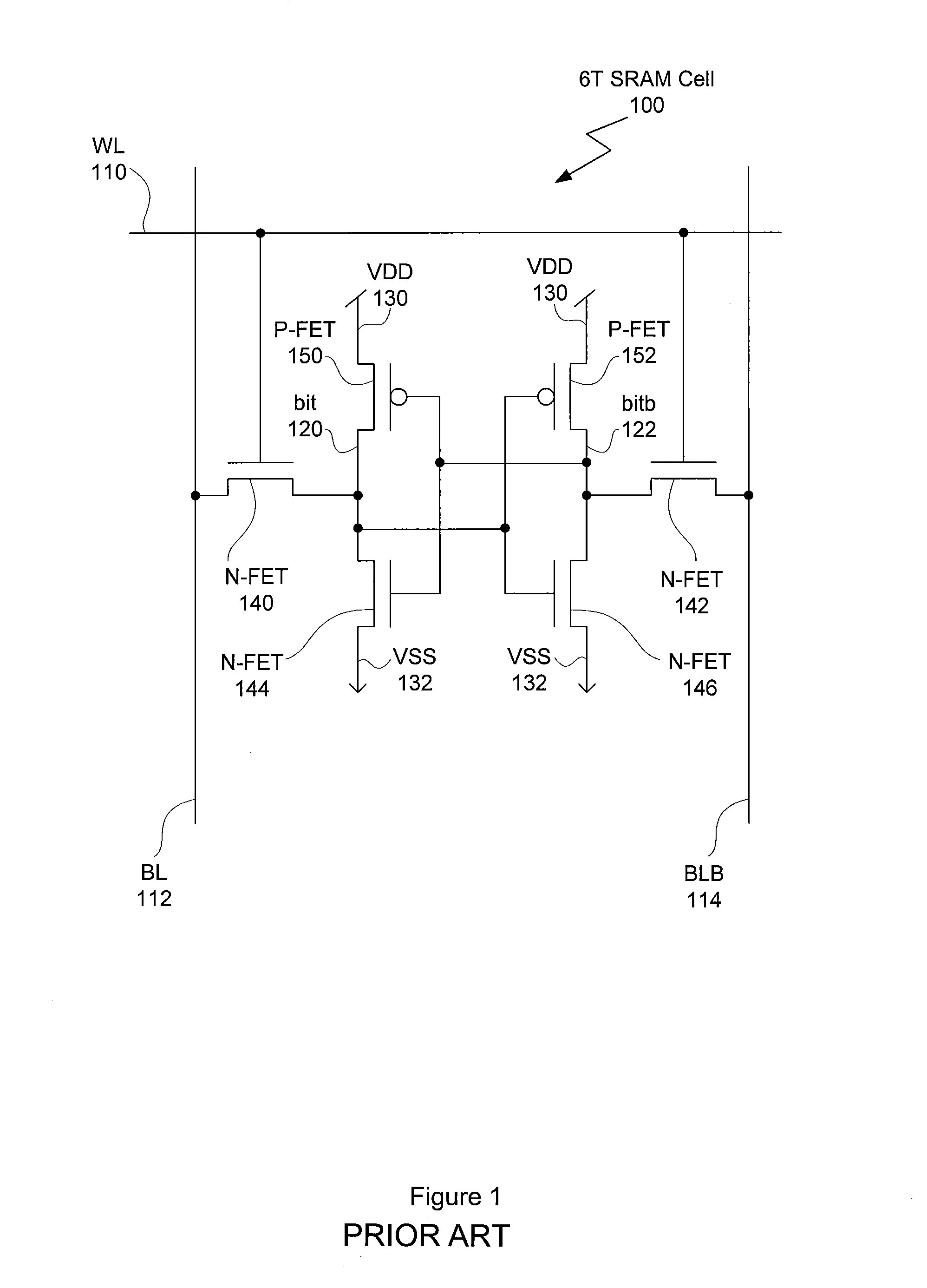
[0021]FIGS. 1 illustrates the circuit design of a six-transistor (6T) static random access memory (SRAM) cell 100, according to one embodiment of the invention. The 6T SRAM cell 100 includes two p-channel field effect transistors (P-FETs) 150, 152, four n-channel field effect transistors (N-FETs) 140, 142, 144 and 146. The 6T SRAM cell is connected to a word line (WL) 110, a bit line (BL) 112, and a bit line bar (BLB) 114.

[0022]P-FET 150 and N-FET 144 form a first logic inverter, with output bit 120. P-FET 152 and N-FET 146 form a second logic inverter, with output bitb 122. P-FETs 150 and 152 are connected to a positive supply voltage, conventionally called “VDD”130 in complimentary symmetry metal-oxide semiconductor (CMOS) circuits. N-FETs 144 and 146 are connected to the zero-voltage reference node (or “ground”), conventionally called “VSS”132 in CMOS circuits. The output of the first logic inverter, bit 120, is connected to the input of the second logic inverter, formed by the g...


PUM


Abstract

One embodiment of the present invention sets forth an active bit line charge keeper circuit for improving the reliability of a static random access memory (SRAM) circuit. The active bit line charge keeper circuit includes two sub-circuits, each disposed between bit line pairs within the SRAM circuit. The first sub-circuit mitigates residual state associated with over-developed read state on the bit lines. The second sub-circuit mitigates the effects of residual state associated with reading one value on a given pair of bit lines and subsequently writing a different value. By mitigating the effects of residual state within an SRAM circuit, higher reliability at a given performance level may be achieved.

Description

BACKGROUND OF THE INVENTION[0001]1. Field of the Invention[0002]Embodiments of the present invention relate generally to static random access memory (SRAM) design and more specifically to an active bit line charge keeper.[0003]2. Description of the Related Art[0004]Integrated circuits commonly embed SRAM circuits to provide on-chip data storage. A given instance of an SRAM circuit typically includes, without limitation, an array of storage cells, write drivers, write column multiplexers, read column selectors, sense amplifiers, and address decoders. One common type of storage cell is a six-transistor (“6T”) storage cell. A two-dimensional array of 6T storage cells allows one selected row of 6T storage cells to be accessed at a time, either for reading or writing data stored in the selected row. Pairs of bit lines typically provide access to data for each column within the row of 6T storage cells. Each pair of bit lines transmits a differential representation of the data stored withi...

Claims


Application Information

Patent Timeline
IPC IPC(8): G11C7/12
CPCG11C11/413G11C7/12
Inventor LIN, HWONG-KWOYANG, GEFRAZIER, ETHAN A.YOUNG, CHARLES CHEW-YUEN
Owner NVIDIA CORP
Why Eureka
Try Eureka