Integrated optocoupler with organic light emitter and inorganic photodetector

a technology of organic light emitters and optocouplers, applied in the direction of diodes, semiconductor devices, electrical apparatus, etc., can solve the problems of high manufacturing cost, difficult integration, and inability to produce both elements on the same substrate, so as to achieve the reduction of oled area, low current consumption, and economic

Inactive Publication Date: 2009-12-01
FRAUNHOFER GESELLSCHAFT ZUR FOERDERUNG DER ANGEWANDTEN FORSCHUNG EV
View PDF12 Cites 7 Cited by
  • Summary
  • Abstract
  • Description
  • Claims
  • Application Information

AI Technical Summary

Benefits of technology

[0024]OLEDs are in particular favourable, since they permit a high integration during a production of optocouplers and can, in addition, be deposited on almost any substrates and can thus, in particular, also be integrated directly on a silicon substrate. Furthermore, a deposition can occur at relatively low temperatures (for example below 100° C.). Thus, OLEDs can be deposited on a normal CMOS / BiCMOS circuit (BiCMOS=Bipolar Complementary Metal Oxide Semiconductor), without any risk of damages. An isolation oxide or an isolation layer present on an integrated circuit (CMOS structure) can simultaneously create an optical connection, i.e. serve as a light guide, whereby a desired electrical isolation value can be adjusted by means of a layer thickness of the isolation layer. Thus, this technology becomes very simple.
[0027]The light emitter and the light receiver have, according to an embodiment of the invention, an “optical proximity” and thus a necessary OLED area can be reduced and a current consumption can be kept low. The production is thus economical. Through an appropriate choice of a wavelength used of the light signal generated (which is substantially determined by the material used), can be achieved as low an absorption as possible of the light guide, which results in an optimized optical signal transmission. In order to maintain a necessary OLED voltage as low as possible, the series of organic layers can have a doped transport layer and a reduced input-voltage threshold can thus be achieved.
[0028]The deposition of the OLED is thus technologically fully compatible with the CMOS / BiCMOS as well as the bipolar technology and thus allows manufacturing integrated OLED optocouplers. A production is even possible without any problem and at low cost on large substrates (e.g. up to 200×200 mm).
[0029]With the OLED technology, i.e. using OLEDs as light emitters, there is provided for the first time the possibility of a monolithically integrated solution for optocouplers, i.e. of performing light generation and detection on one substrate (e.g. on a silicon substrate). They thus offer advantages as regards the size of the components as wells as regards the possibility of integrating new functions, i.e. they are can be easily and highly integrated. In addition, they exhibit high efficiency at varying insulation resistances and have low power consumption.
[0031]The advantages of the optocouplers with integrated OLEDs, compared with well-known hybrid solutions, can be summarized as follows. The complexity of the construction and connection technique (CCT) for the integration is reduced and the costs are reduced. In addition, the monolithic integration of light source, electrical insulator, light guide and photodetector on a chip can easily be implemented. Furthermore, standard CMOS layers / structures can be used as electrical insulator and light guide. This results into an improvement of the isolation strength when using a SOI-CMOS substrate and a reduction of the chip area. Finally, the exemplary embodiments of the present invention provide the possibility of a complex integration of an activation circuit for the light emitter and electronic reading unit for the photodetector.

Problems solved by technology

Since conventional LEDS, as has been said, primarily use III-V semiconductors and the detector circuit (i.e. the photodetector 50 and the activating circuit) is mostly based on silicon, both elements cannot be produced on the same substrate and an integration therefore proves difficult.
A possible hybrid integration in optocouplers, such as known for example from the state of the art, necessitates in principle a higher manufacturing cost and, as a matter of fact, does not allow a general price regression with large numbers of units.
Furthermore, because of the hybrid structure, the necessary reliability for car applications can be achieved only at an extremely high cost.

Method used


Image

  • Integrated optocoupler with organic light emitter and inorganic photodetector
  • Integrated optocoupler with organic light emitter and inorganic photodetector
  • Integrated optocoupler with organic light emitter and inorganic photodetector

Examples


Embodiment Construction

[0044]Before describing the present invention more in detail hereafter with reference to the drawings, the attention is drawn on the fact that same elements in the figures are designated by same or similar reference numerals, and that a repeated description of these elements is omitted.

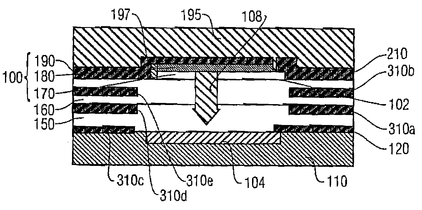
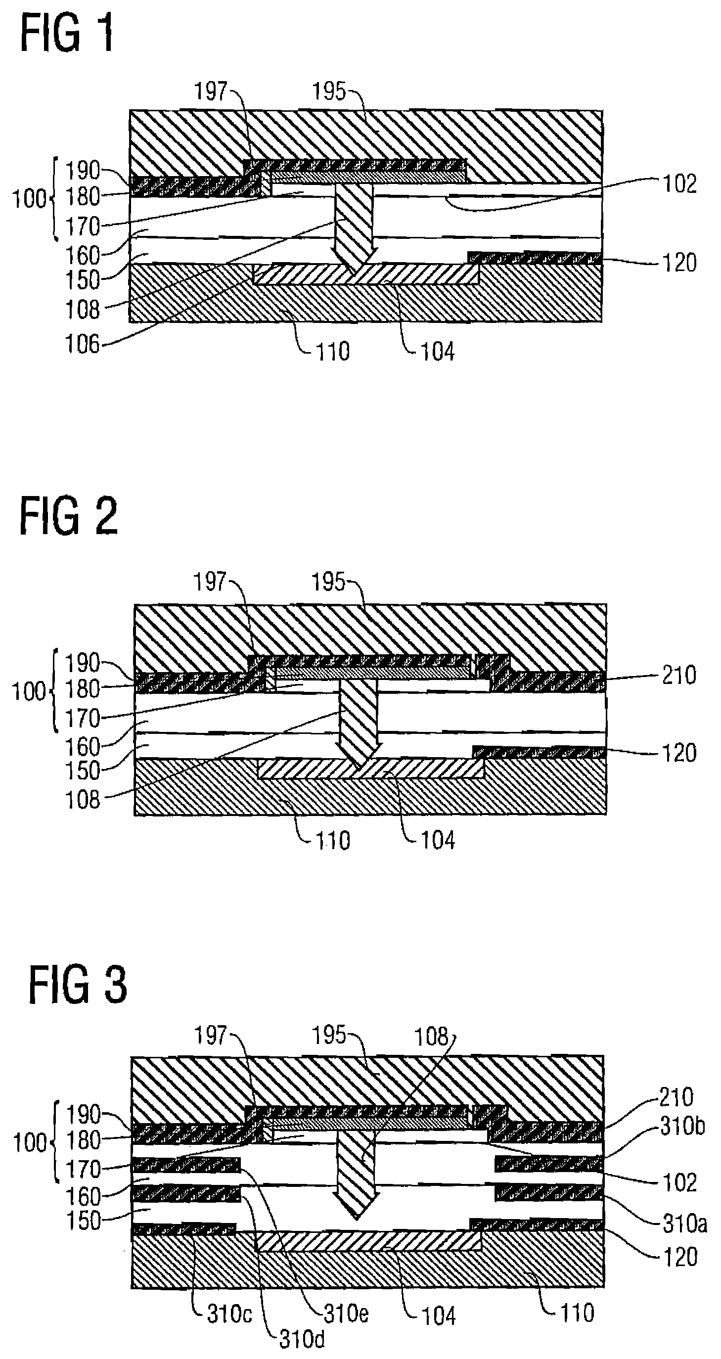
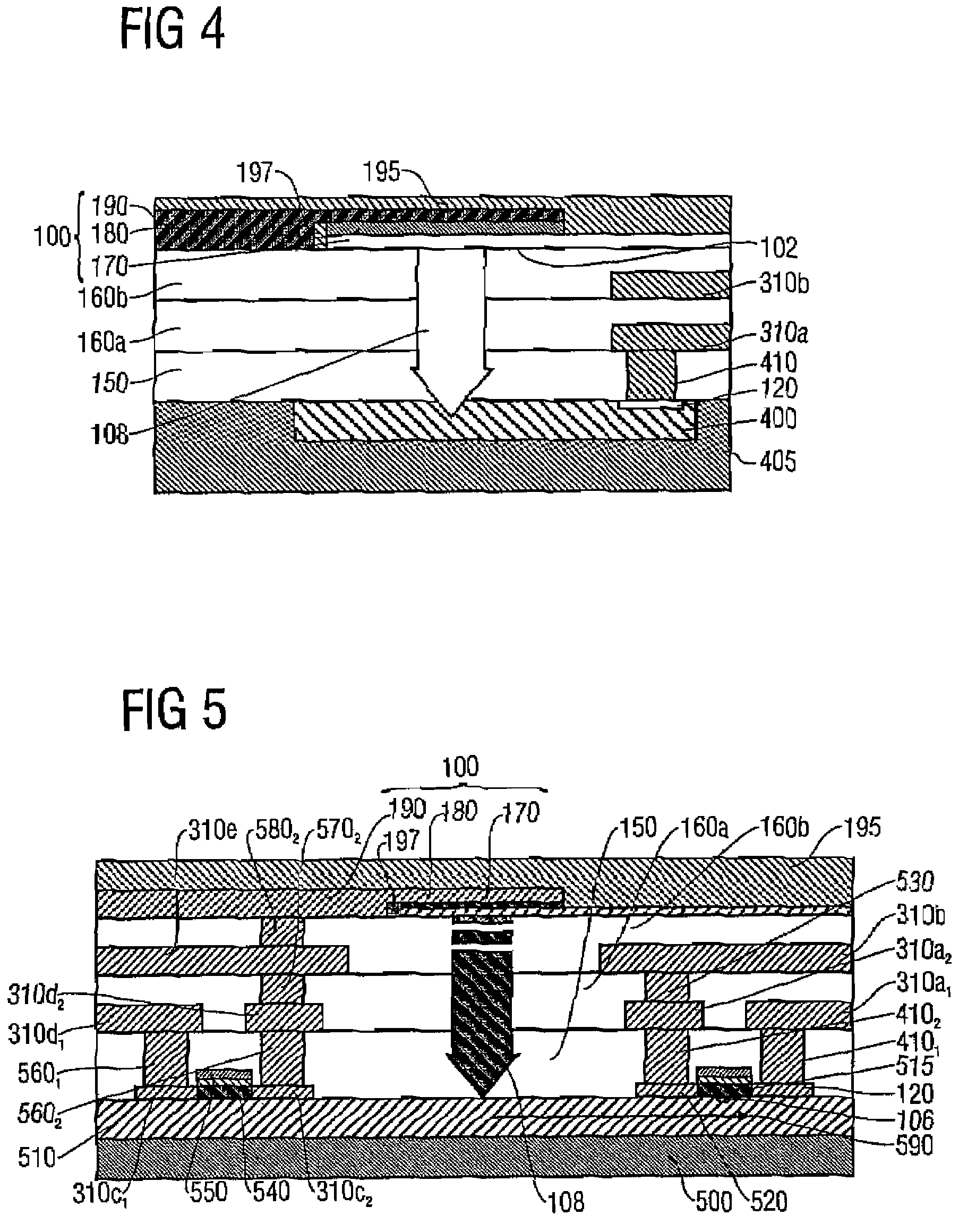
[0045]FIG. 1 shows an OLED 100 as a bottom emitter, which has a light-emitting surface 102 and radiates directly onto the photodetector 104 located under it, which is for example part of a CMOS structure. The photodetector 104 is embedded in a substrate 110, is connected through a contact 120 and shielded by an ILD layer 150 of the CMOS structure. An IMD layer 160 of the CMOS structure serves as a basis or substrate for the OLED 100, i.e. on the IMD layer 160 are deposited a transparent electrode 170, a series of organic layers 180 and a second electrode 190. A passivation or protective layer 195 serves as finishing layer and a side passivation 197 isolates the transparent electrode 170 from the secon...


PUM


Abstract

An optocoupler has an organic light emitter and an inorganic photodetector with a detector area, the detector area being optically coupled to the organic light emitter. The organic light emitter converts an electrical input signal into a light signal and the inorganic photodetector converts the light signal into an electrical output signal, the organic light emitter and the inorganic photodetector being integrated in a component and galvanically separated.

Description

CROSS-REFERENCE TO RELATED APPLICATION[0001]This application claims priority from German Patent Application No. 10 2006 040 788.1, which was filed on Aug. 31, 2006, and is incorporated herein by reference in its entirety.BACKGROUND OF THE INVENTION[0002]1. Field of the Invention[0003]The present invention refers to an integrated optocoupler with an organic light emitter and an inorganic photodetector, and in particular to a monolithically integrated CMOS optocoupler with an OLED light source.[0004]2. Description of the Related Art[0005]Optocouplers have been widely spread as technical means for galvanic isolation and / or electrical potential separation. This includes applications in car industry, consumer electronics, medical and measuring technology, data communication and the like. Optocouplers are used for electrical isolation of an input signal from a corresponding output signal and can be used as a substitution for relays and Reed relays (protective glass relays). They are advan...

Claims


Application Information

Patent Timeline
Patent Type & Authority Patents(United States)
IPC IPC(8): H01L27/142
CPCH01L27/3227H01L31/12H01L51/5284H10K59/60H10K50/865
Inventor VOGEL, UWEAMELUNG, JOERG
Owner FRAUNHOFER GESELLSCHAFT ZUR FOERDERUNG DER ANGEWANDTEN FORSCHUNG EV
Why Eureka
Try Eureka