
Differential amplifier, digital-to-analog converter, and display device

a technology of digital to analog converter and display device, applied in the direction of code conversion, static indicating device, instruments, etc., can solve the problems of reduced voltage between adjacent gray scale levels, increased die cost, and increased decoder area, and achieve low power, high accuracy output, and high accuracy output

Inactive Publication Date: 2009-11-24
NEC CORP
View PDF7 Cites 8 Cited by
  • Summary
  • Abstract
  • Description
  • Claims
  • Application Information

AI Technical Summary

Benefits of technology

The present invention provides a differential amplifier that can output a large number of output levels using the less number of levels. This is achieved by canceling out multiple gray scale levels using a single differential pair of transistors. The amplifier has high accuracy output and reduces power consumption. It also includes a data output period with two periods for improved accuracy. The invention can be used in digital-to-analog converters and display devices to achieve high-accuracy output and reduce decoder area. The technical effects of the invention include reducing the number of gray scales needed, reducing the number of transistors required, and improving accuracy output.

Problems solved by technology

Further, there is a problem that the number of transistors for selecting gray scale voltages also increases, and the decoder area increases, so that die cost increases (first problem).
There is also a problem that with the progress of multiple gray scale levels, a voltage between adjacent gray scale levels is reduced, so that more accurate output is required (second problem).
Thus, there is a problem that power consumption increases more than in the case of one differential pair (third problem).
However, the amplifiers in Patent Document 1 and Patent Document 2 cannot solve the first problem of the increase in the die cost caused by the creation of multiple gray scales.

Method used


Image

  • Differential amplifier, digital-to-analog converter, and display device
  • Differential amplifier, digital-to-analog converter, and display device
  • Differential amplifier, digital-to-analog converter, and display device

Examples


Embodiment Construction

[0152]The preferred embodiments of the present invention will be described below with reference to appended drawings. same reference symbols in respective drawings are assigned to same constituent elements.

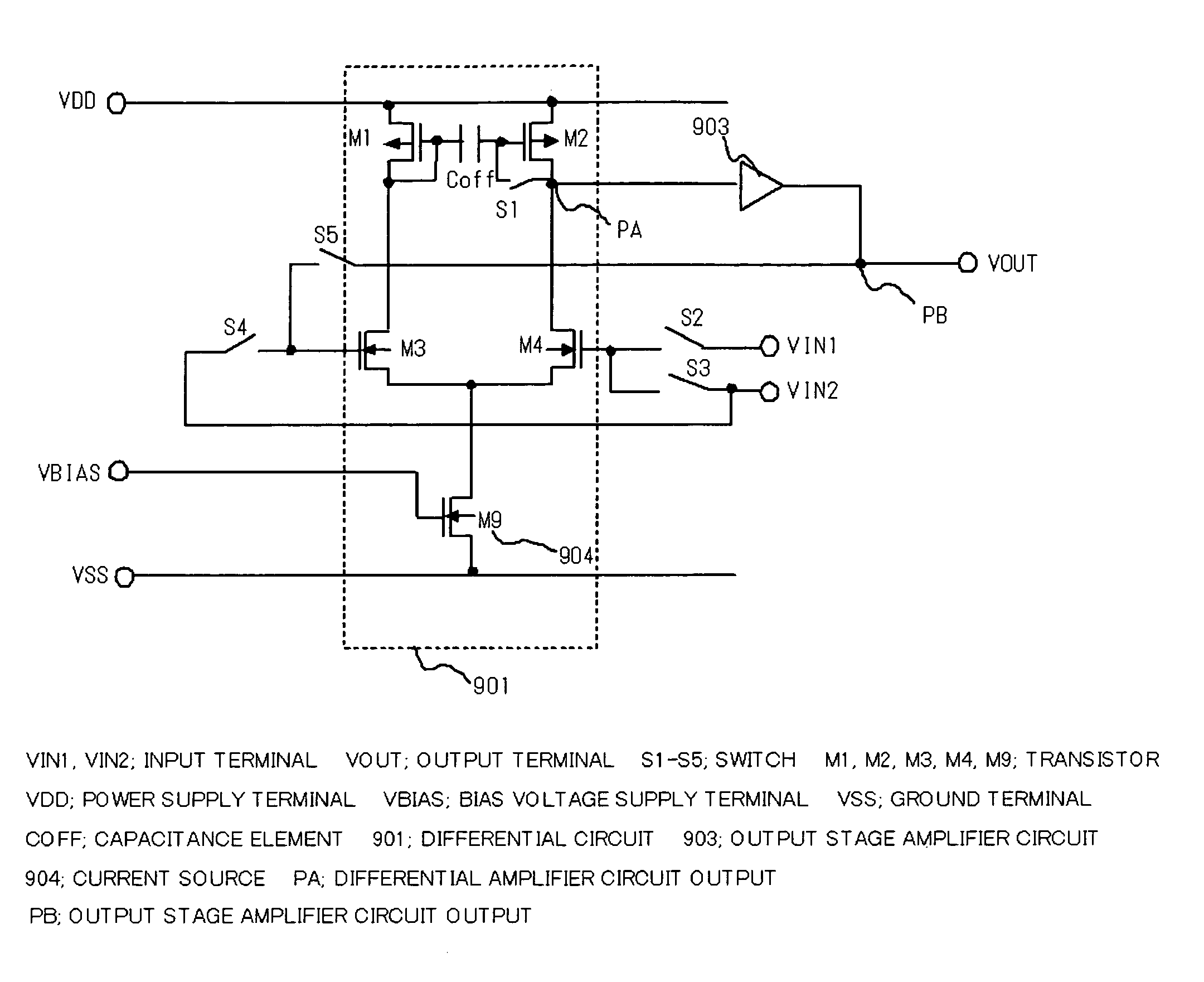
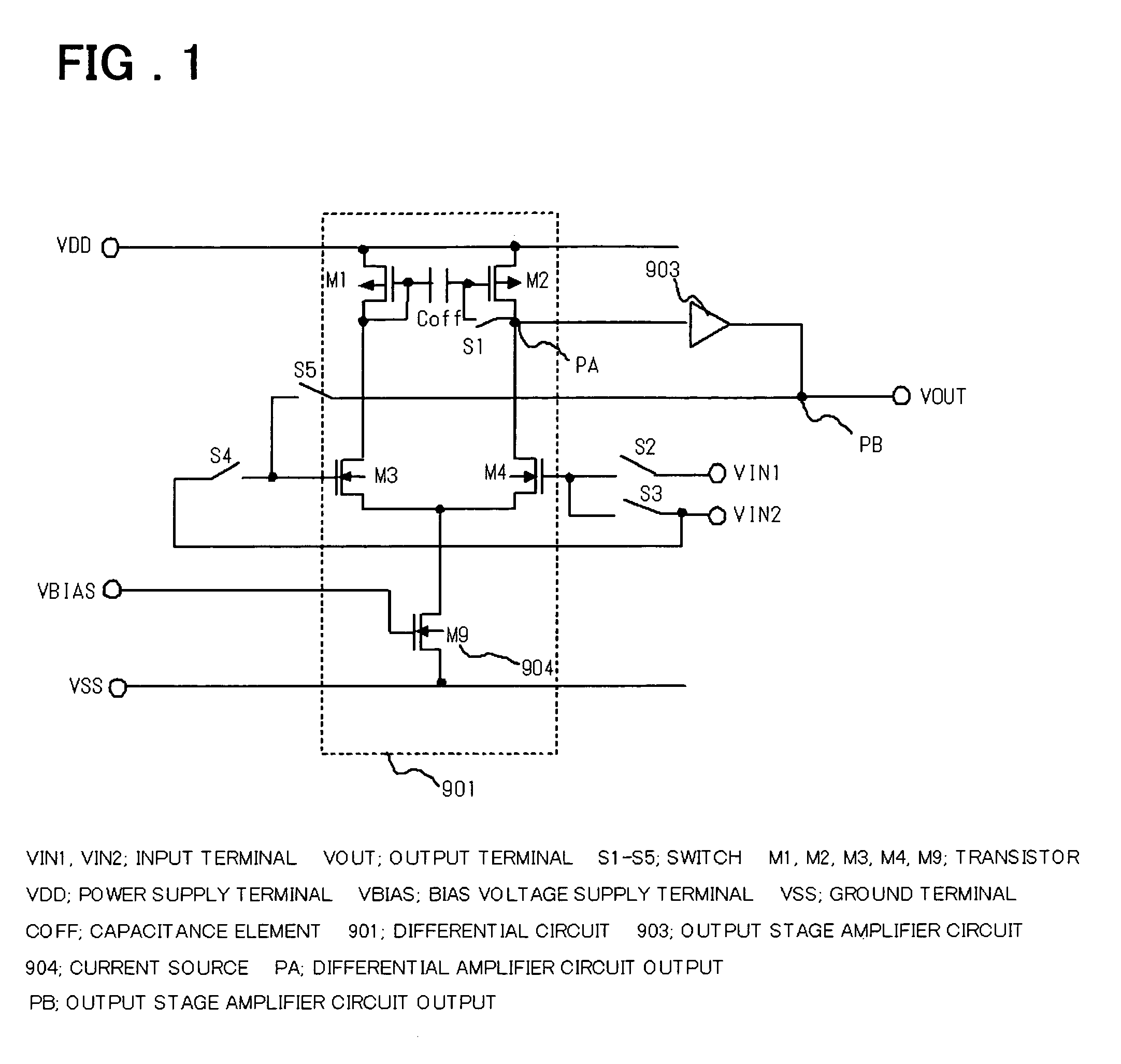
[0153]A circuit configuration according to a first embodiment of the present invention will be described below. FIG. 1 is a diagram showing a configuration of a differential amplifier according to the first embodiment of the present invention. Referring to FIG. 1, the differential amplifier according to the present embodiment includes a differential pair (constituted from transistors M3 and M4) which is driven by a current source 904 (a transistor M9 with a bias voltage supplied thereto), a load circuit to which the outputs of the differential pair is connected, and an output stage amplifier circuit 903 that receives a differential output signal. The load circuit is constituted from transistors M1 and M2. Drains of the transistors M1 and M2 are connected to drains of the transisto...


PUM


Abstract

Disclosed is a differential amplifier of a multi-level output type comprising a load circuit including a diode-connected first transistor with a source thereof connected to a power supply and a second transistor with a source thereof connected to the power supply and connected to a gate of the first transistor through a capacitor, a differential pair including a third transistor and a fourth transistor with sources thereof connected in common and drains thereof connected to drains of the first and second transistors, respectively, a current source for supplying a current to the differential pair, a first switch connected between a gate of the second transistor and a drain of the fourth transistor, an amplifier with an input thereof connected to a drain of the second transistor and an output thereof connected to an output terminal, a second switch connected between a gate of the fourth transistor and a first input terminal, a third switch connected between the gate of the fourth transistor and a third input terminal, a fourth switch connected between a gate of the third transistor and a second input terminal, and a fifth switch connected between the gate of the third transistor and the output terminal. Switching control between a first state where the first, second and fourth switches are turned on and the third and fifth switches are turned off and a second state where the first and second fourth switches are turned off and the third and fifth switches are turned on is performed.

Description

FIELD OF THE INVENTION[0001]The present invention relates to a differential amplifier, a digital-to-analog converter, and a display device. More specifically, the invention relates to a differential amplifier suitable for use as the differential amplifier of a multi-level output type having an offset canceling function, and a digital-to-analog converter and a display device both having the differential amplifier.BACKGROUND OF THE INVENTION[0002]As a conventional typical data driver that drives a data line in a liquid crystal display device, a configuration as shown in FIG. 22 is employed. Referring to FIG. 22, this data driver includes a shift register 209, a data register 208, a data latch 207, a level shifter 206, a gray scale voltage generation circuit 205, decoders 203, and an output circuit 202 (amplifiers 201).[0003]An operation of the data driver shown in FIG. 22 will be described. The shift register 209 outputs a shift pulse responsive to a clock signal CLK. The data registe...

Claims


Application Information

Patent Timeline
Patent Type & Authority Patents(United States)
IPC IPC(8): H03M1/66
CPCG09G3/3688H03F3/45183G09G2310/027H03F2203/45616H03M1/765H03F2203/45656H03F2203/45682H03F2203/45728H03F2203/45631
Inventor IRIGUCHI, MASAOTSUCHI, HIROSHI
Owner NEC CORP
Learn More