
Method and arrangement for performing analog signal processing and measuring between a signal source and a load

a technology of analog signal processing and measuring between a signal source and a load, applied in the direction of waveguide type devices, digital transmission, modulation, etc., can solve the problems of difficult to realize a transmission line having an electrical length of 90 degrees, and the number of electrical components needed to realize a 6 cm transmission line for the elements shown in fig. 1

Active Publication Date: 2009-11-17
NOKIA TECH OY
View PDF5 Cites 7 Cited by
  • Summary
  • Abstract
  • Description
  • Claims
  • Application Information

AI Technical Summary

Benefits of technology

This approach reduces component costs, production and quality control costs, and physical space requirements, while minimizing power losses and enabling easier miniaturization of communication devices.

Problems solved by technology

In many applications it is difficult to realize a transmission line having an electrical length of 90 degrees at a center frequency of a signal to be conducted via the transmission line.
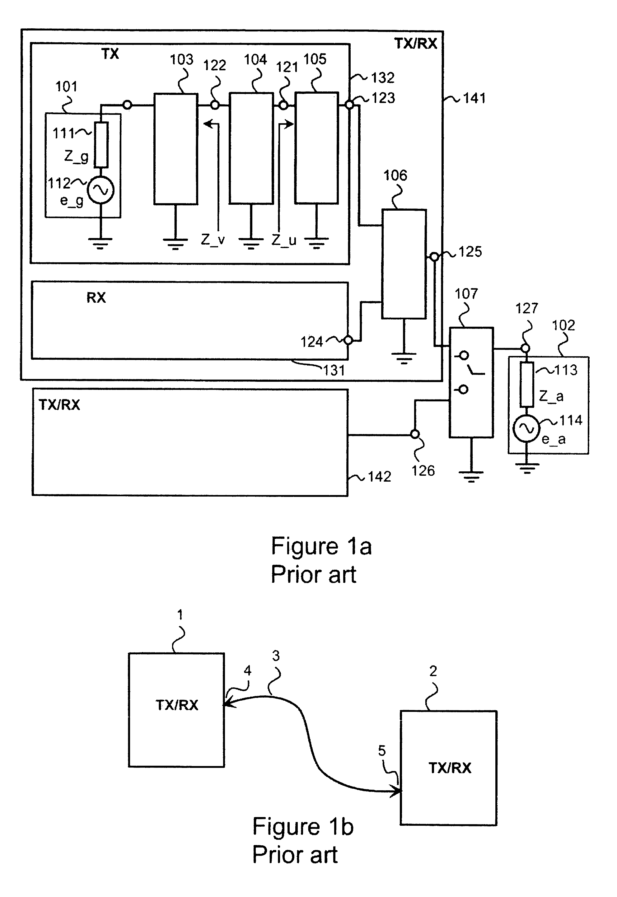
For e.g. a mobile communication device it is very difficult to realize 6 cm transmission lines for the elements shown in FIG. 1a.
A problem of transmitters, receivers, and receiver-transmitters according to prior art, like the receiver-transmitter shown in FIG. 1a, is the fact that a number of electrical components needed for realizing a sensor element, an impedance transformer, a filter, a duplexer filter, and a throw-over switch is quite high.
High number of electrical components means high component costs of products, expensive production and quality control routines, need for physical space making miniaturizing of products difficult, and power losses.
In other words, individual elements of a system can be good but the system as a whole can be poor.

Method used


Image

  • Method and arrangement for performing analog signal processing and measuring between a signal source and a load
  • Method and arrangement for performing analog signal processing and measuring between a signal source and a load
  • Method and arrangement for performing analog signal processing and measuring between a signal source and a load

Examples


Embodiment Construction

[0089]FIGS. 1-7 have been explained above in the description of the prior art.

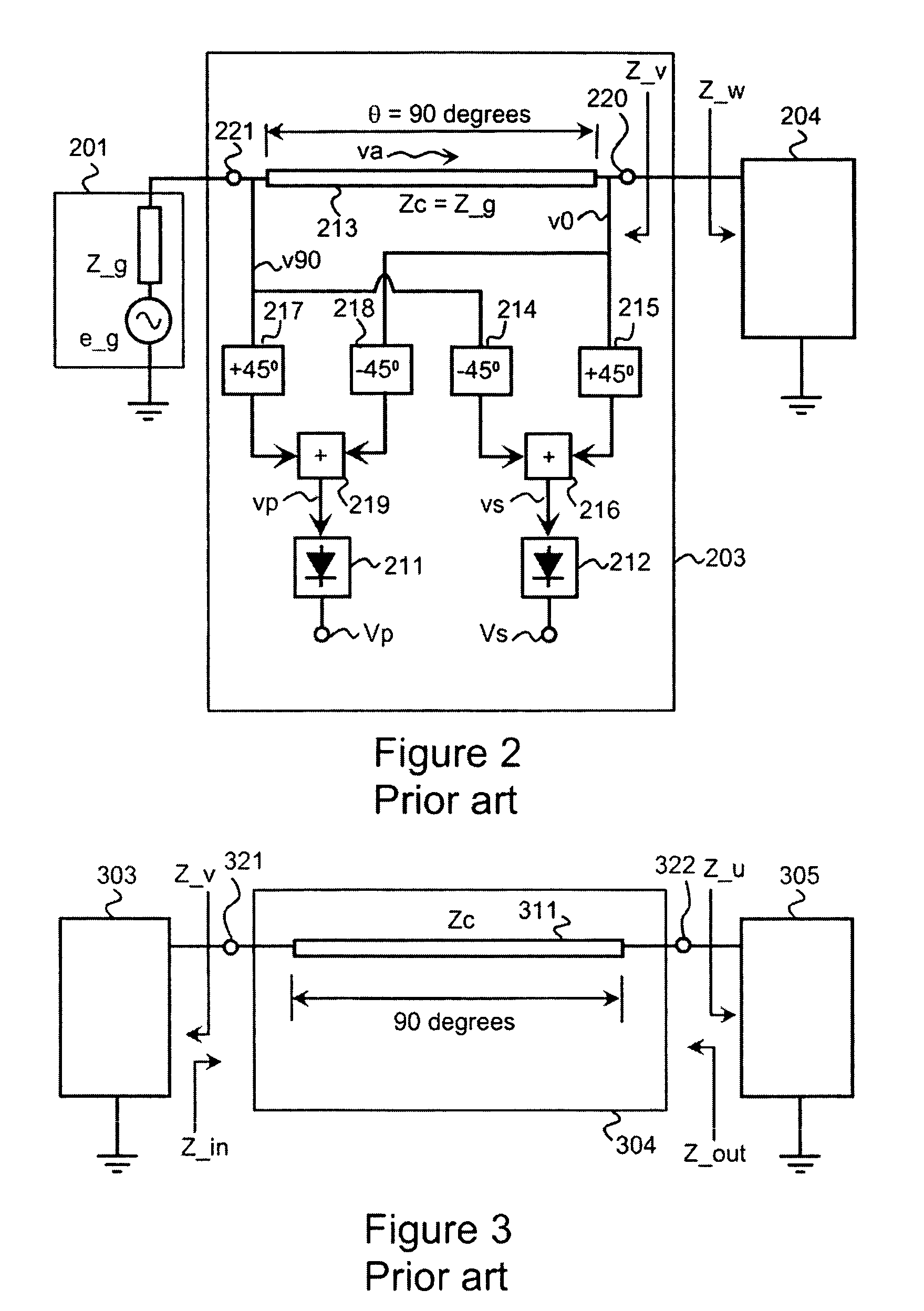
[0090]FIG. 8a shows a combined sensor element and impedance transformer 803 according to an embodiment of the invention in which one 90 degrees phase shifter is used as a part of a sensor element and also as a quarter-wave impedance transformer. In this embodiment of the invention the 90 degrees phase shifter is realized with a transmission line 813 having an electrical length of 90 degrees at a center frequency of a signal e_g. A wave impedance Zc of the transmission line is chosen so that there is an impedance matched situation, i.e. an impedance Z_y is sufficiently near to a generator impedance Z_g. This is accomplished by choosing:

Zc=√{square root over (Z—g×Z—w)},  (10)

where Z_w is an input impedance of a system 804 loading the combined sensor element and impedance transformer 803. A reflection coefficient ρ in respect of the wave impedance is

[0091]ρ=Z_w-ZcZ_w+Zc.(11)

[0092]In the impedance matched situ...


PUM


Abstract

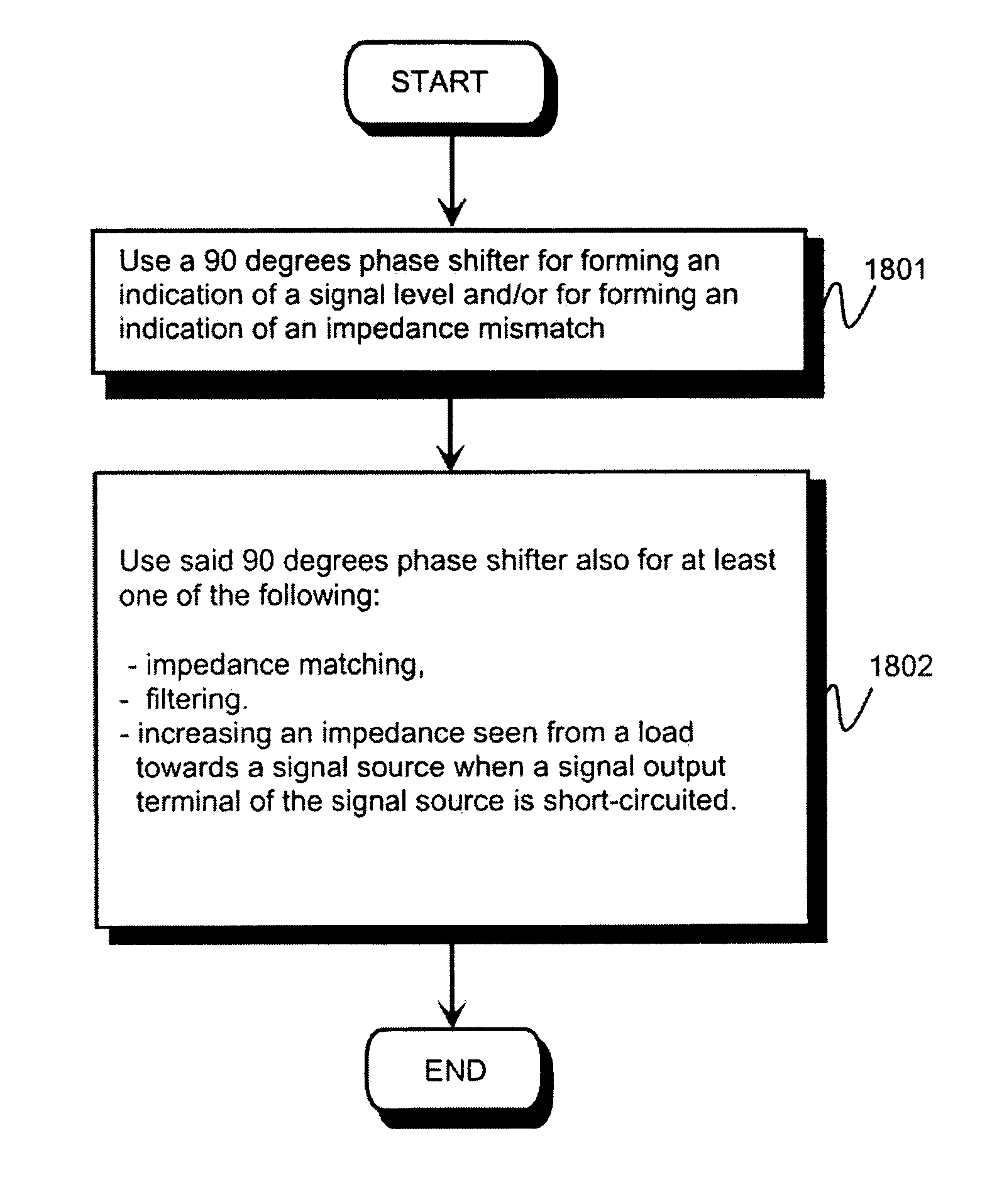
A method and arrangement is shown for performing analog signal processing tasks like impedance matching, phase shifting, and / or signal filtering on a signal path from a signal source to a load so that a number of electrical components is smaller than that of solutions according to prior art for performing corresponding analog signal processing tasks. The signal source can be e.g. a power amplifier of a transmitter and the load can be e.g. an antenna of the transmitter. A solution is shown in which a same ninety degree phase shifter element (910) is used for performing more than one of the analog signal processing tasks of the kind mentioned above.

Description

FIELD OF THE INVENTION[0001]The invention relates to analog signal processing in communicating devices. The invention especially relates to a method and arrangement for performing analog signal processing tasks like impedance matching, phase shifting, and / or signal filtering on a signal path from a signal source to a load. The signal source can be e.g. a power amplifier of a transmitter and the load can be e.g. an antenna of the transmitter.BACKGROUND OF THE INVENTION[0002]In an electrical system including a signal source that produces an analog signal and a load circuit that delivers the analog signal out from the system analog signal processing is often needed in a signal path between the signal source and the load circuit. The signal source can be, for example, a power amplifier of a transmitter and the load circuit can be, for example, an antenna or a line transformer of the transmitter. The analog signal processing can comprise impedance transformation in order to match an outp...

Claims


Application Information

Patent Timeline
Patent Type & Authority Patents(United States)
IPC IPC(8): H03C1/52
CPCH01P1/18H04B1/0466H04B2001/0416
Inventor VAISANEN, RISTO
Owner NOKIA TECH OY
Learn More